A power semiconductor module packaging structure and packaging method

A power semiconductor and module packaging technology, which is applied in the direction of semiconductor devices, semiconductor/solid-state device manufacturing, semiconductor/solid-state device components, etc., can solve the difficulty in processing anti-corrosion films or coatings, increase the size of power modules, and unfavorable product size issues such as miniaturization, to achieve the effects of small deformation, low module thermal resistance, and high reliability

Active Publication Date: 2019-11-26
WUXI LEAPERS SEMICON CO LTD
View PDF4 Cites 0 Cited by
  • Summary
  • Abstract
  • Description
  • Claims
  • Application Information

AI Technical Summary

Problems solved by technology

In this way, if a metal layer with a thickness of 1mm is used, in order to ensure a 1mm insulation distance, the gap between the top metal layers may reach 1.8mm. If a metal layer with a thickness of 3mm is used, in order to ensure a 1mm insulation distance, the gap between the top metal layers The broadband may reach 5.4mm, such a large bandwidth will make the power module larger, which is not conducive to the miniaturization of the product
The second problem is that in the corrosion process, it is generally necessary to protect the place that does not need to be corroded with an anti-corrosion film or coating. It is relatively easy for a relatively thin metal bottom (below 3mm) plate with a flat bottom surface, but for picture figure 2 The bottom surface shown is a Pinfin or other shaped metal bottom plate or like image 3 As shown in the metal base plate with water channels, the complex structure and large thickness make it extremely difficult to process the anti-corrosion film or coating

Method used


Image

  • A power semiconductor module packaging structure and packaging method
  • A power semiconductor module packaging structure and packaging method
  • A power semiconductor module packaging structure and packaging method

Examples


Embodiment Construction

[0059] The specific embodiments of the present invention will be described in further detail below in conjunction with the accompanying drawings of the specification.

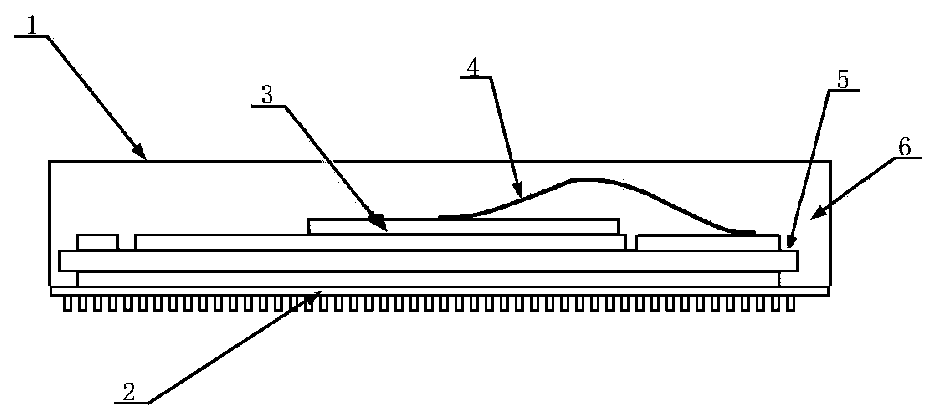
[0060] The present invention designs a power semiconductor module packaging structure. In practical applications, it specifically includes a metal bottom plate 2, a base layer, a power semiconductor chip 3, and a metal bonding wire 4; the base layer includes a thermally conductive insulating resin film 11 and a metal circuit layer 12. Wherein, the thermally conductive insulating resin film 11 contains boron nitride fillers, the metal circuit layer 12 is provided on the upper surface of the thermally conductive insulating resin film 11, the lower surface of the thermally conductive insulating resin film 11 is provided on the upper surface of the metal base plate 2, and the power semiconductor chip 3 Set on the upper surface of the metal circuit layer 12; one end of the metal bonding wire 4 is connected to the upper ...


PUM


Abstract

The invention relates to a power semiconductor module packaging structure and a packaging method thereof. A resin or other curable material is injected into a gap of a specially processed metal circuit layer and then solidification is carried out; the metal circuit layer and a heat-conducting insulating resin film are pressed on a metal bottom plate; and bubbles in the gap of the metal circuit layer and in the heat-conducting insulating resin film are removed and solidified by using the solidified material, so that the insulation property is ensured. Or bubbles in the heat-conducting insulating resin film are removed and solidified by using the solidification process of the plastic-packaging resin in the plastic-packaging process, so that the insulation property is ensured. Therefore, themetal circuit layer with the small gap and the large thickness can be formed on the heat-conducting insulating resin film even when a Pinfin metal bottom plate, a metal bottom plate with one side being a non-plane surface, or a metal bottom plate with a water-cooled flow path inside. The module based on the structure has advantages of low thermal resistance, small deformation and high reliability.

Description

Technical field [0001] The invention relates to a power semiconductor module packaging structure and packaging method, and belongs to the technical fields of power semiconductor module packaging, motor drives, and power electronic converters. Background technique [0002] In the application of power supplies and power electronic converters, power semiconductors (IGBT, MOSFET, SiC, GaN, etc.) are widely used, and module packaging is generally used in high-power situations. The occasions where the heat of power semiconductor devices is more serious, such as the motor drive in electric vehicles, generally adopt a water-cooled package. Packaging forms that are now widely used such as figure 1 As shown, the power module is mainly composed of a metal bottom plate (in industrial applications, the bottom surface of the metal bottom plate is generally flat, and in automotive applications, it is mostly in the form of Pinfin with metal pillars or other forms of non-planar heat dissipation s...

Claims


Application Information

Patent Timeline
Patent Type & Authority Patents(China)
IPC IPC(8): H01L23/31H01L21/56
CPCH01L21/56H01L23/31H01L2224/48091H01L2924/00014
Inventor 葛小华
Owner WUXI LEAPERS SEMICON CO LTD
Why Eureka
Try Eureka