An array substrate and display device
A technology for array substrates and display areas, which is applied to semiconductor devices, electrical components, circuits, etc., can solve problems such as affecting display quality and increasing wiring resistance, so as to improve display quality, reduce overlap resistance, and avoid cathode overlap The effect of the area of influence
- Summary
- Abstract
- Description
- Claims
- Application Information
AI Technical Summary
Problems solved by technology
Method used
Image

Examples
Embodiment 1
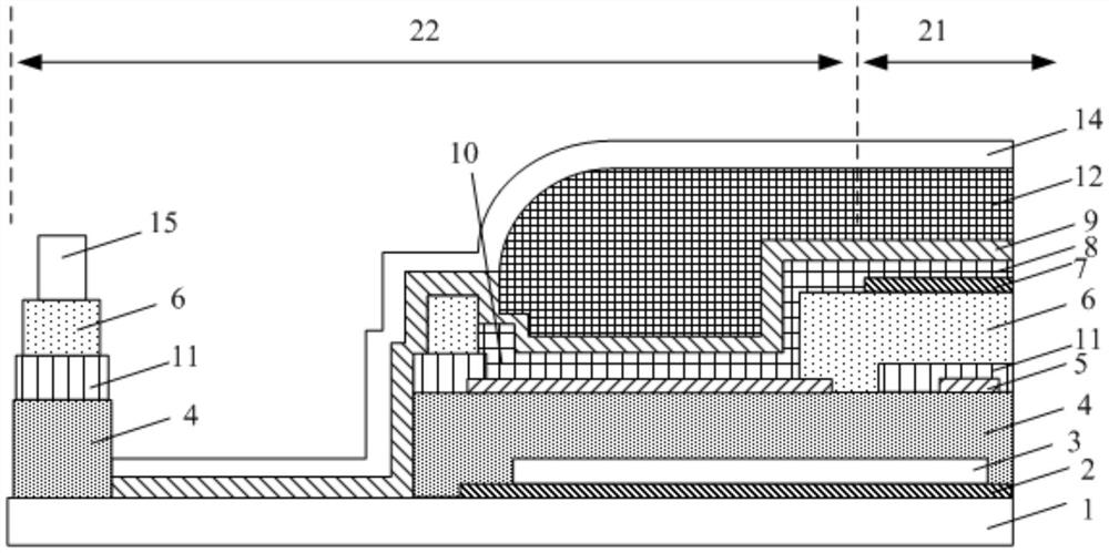
[0034] This embodiment aims at the problem that the narrow frame design compresses the overlapping area of the cathode and the connecting wiring in the edge area, resulting in a decrease in display quality, and provides an array substrate. The overlap is set as a concave-convex zigzag surface connection to obtain a better narrow-frame cathode overlap structure, so that when the width of the cathode and the connecting trace is constant, the overlap area between the cathode and the connecting trace is guaranteed and the lap resistance is reduced. to improve display quality.
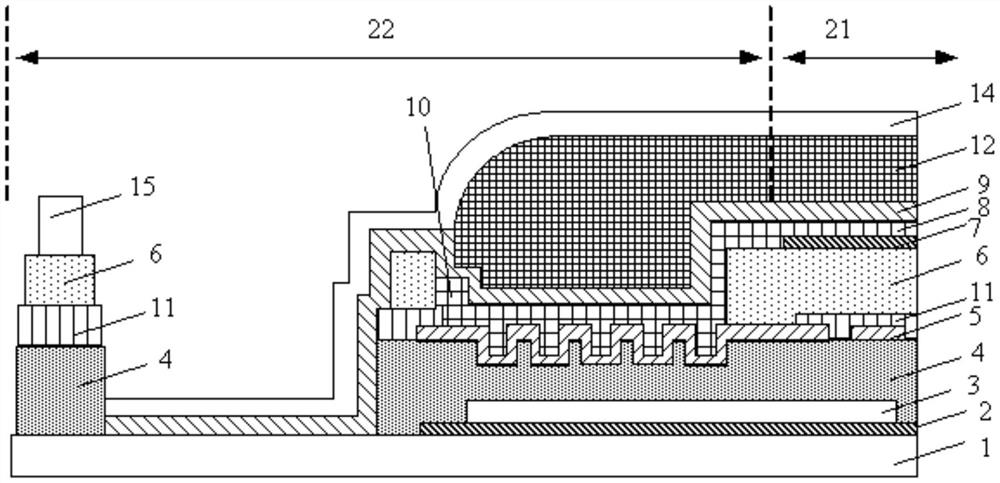
[0035] like figure 1 As shown, the array substrate includes a display area 21 and a non-display area 22 located on the periphery of the display area 21. The display area 21 includes a plurality of pixel structures, and the lead-out lines 10 of the pixel structures are overlapped with the connecting wires 5, and the connecting wires 5 are used for In the receiving signal supply circuit (located in figure...
Embodiment 2
[0050] This embodiment provides an array substrate, which can ensure the overlapped area of the cathode and the connecting wires under the condition that the widths of the lead-out wires of the cathode and the connecting wires are constant, so as to improve the display quality.
[0051] Different from Embodiment 1, the array substrate in this embodiment is also provided with the same layer as the anode and the auxiliary connection line formed of the same material as the anode.
[0052] like Figure 4 As shown, in the area where the connecting wire 5 and the lead-out wire 10 overlap, an auxiliary connecting wire 13 is provided between the connecting wire 5 and the lead-out wire 10 , and the auxiliary connecting wire 13 is in direct contact with the connecting wire 5 . By adding the auxiliary connection line 13, the impedance value can be further reduced.
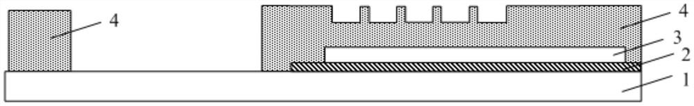
[0053] It is easy to understand that the auxiliary connecting wire 13 and the connecting wire 5 have a concave-convex st...
Embodiment 3
[0059] This embodiment provides an array substrate, which can ensure the overlapping area of the lead-out wire of the cathode and the connecting wire when the width of the cathode and the connecting wire is constant, so as to improve the uniformity of pixel brightness.
[0060] like Figure 5 As shown, compared with the array substrate in the first embodiment, the array substrate in this embodiment is further provided with a second passivation layer 16 above the driving circuit 3 . The second passivation layer 16 can better protect the driving circuit 3 and improve reliability. It is easy to understand that, the second passivation layer 16 may also be disposed above the driving circuit 3 of the array substrate in the second embodiment.
[0061] The array substrate of this embodiment is suitable for a narrow frame structure using a double-layer passivation layer, which can provide better protection for the driving circuit.
PUM
 Abstract
Description
Claims
Application Information
 - R&D
- Intellectual Property
- Life Sciences
- Materials
- Tech Scout
- Unparalleled Data Quality
- Higher Quality Content
- 60% Fewer Hallucinations
Browse by: Latest US Patents, China's latest patents, Technical Efficacy Thesaurus, Application Domain, Technology Topic, Popular Technical Reports.
© 2025 PatSnap. All rights reserved.Legal|Privacy policy|Modern Slavery Act Transparency Statement|Sitemap|About US| Contact US: help@patsnap.com