A display substrate, manufacturing method thereof, and display device

A technology for a display substrate and a manufacturing method, which is applied in the fields of instruments, computing, electrical and digital data processing, etc., can solve the problems of TFT-LCD moiré, affecting the display visual effect, light diffraction phenomenon, etc., so as to avoid moiré and improve display vision. effect, the effect of avoiding diffraction

Active Publication Date: 2021-08-24
BOE TECH GRP CO LTD +1
View PDF8 Cites 0 Cited by
  • Summary
  • Abstract
  • Description
  • Claims
  • Application Information

AI Technical Summary

Problems solved by technology

The disadvantage of this kind of TFT-LCD is that since the black matrix 10 and the slits 31 on the touch electrodes 30 are arranged regularly, when the light passes through the layer where the black matrix 10 is located, regular parallel light is formed. When the slit 31 of the control electrode 30 is connected, the diffraction phenomenon of light will occur, which will cause moiré phenomenon in TFT-LCD, thus affecting the display visual effect

Method used


Image

  • A display substrate, manufacturing method thereof, and display device
  • A display substrate, manufacturing method thereof, and display device
  • A display substrate, manufacturing method thereof, and display device

Examples


Embodiment Construction

[0034] In order to make the purpose, technical solutions and advantages of the embodiments of the present invention more clear, the following will clearly and completely describe the technical solutions of the embodiments of the present invention in conjunction with the drawings of the embodiments of the present invention. Apparently, the described embodiments are some, not all, embodiments of the present invention. All other embodiments obtained by those skilled in the art based on the described embodiments of the present invention belong to the protection scope of the present invention.

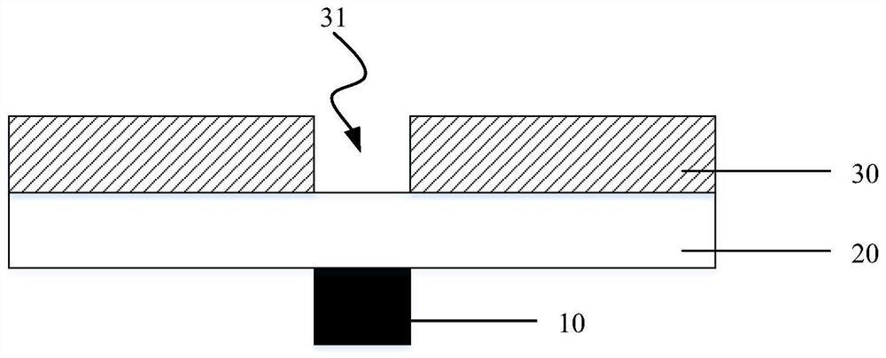
[0035] Please refer to Figure 10 , Figure 13 to Figure 15 , an embodiment of the present invention provides a display substrate, including:

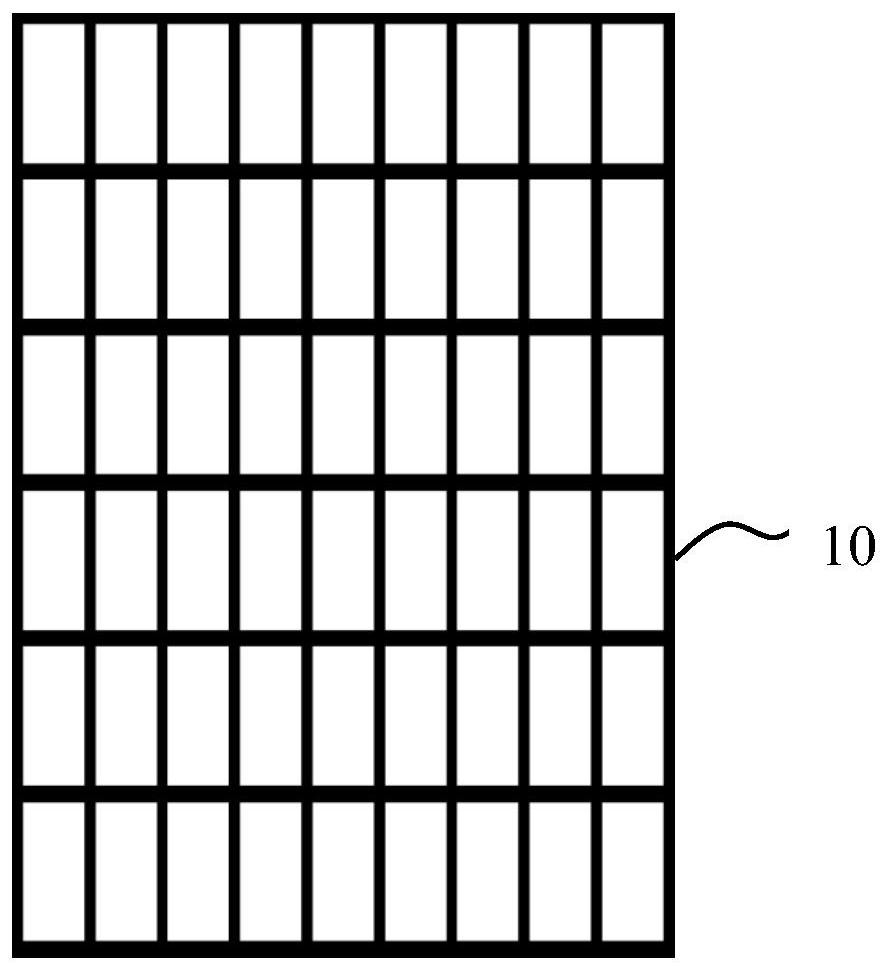
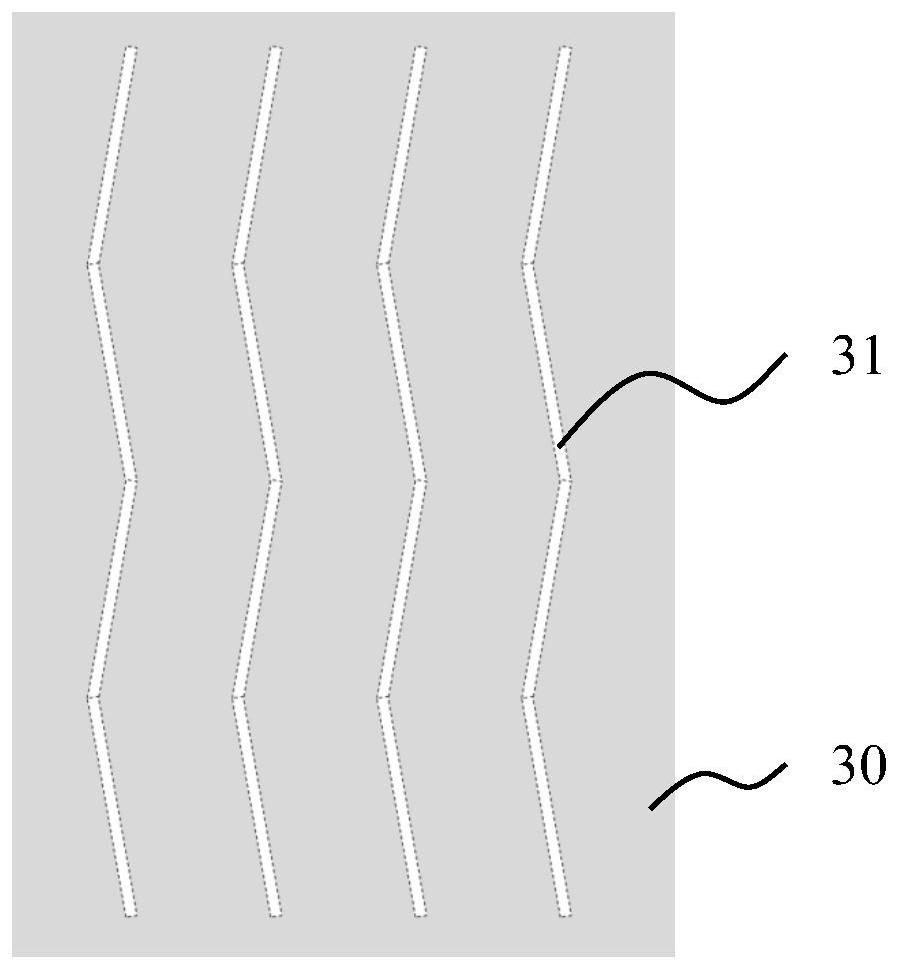
[0036] The base substrate 120, and the black matrix 110, the scattering layer and a plurality of mutually insulated touch electrodes 140 arranged on the base substrate 120, each of the touch electrodes 140 is provided with at least one slit 141, ...


PUM


Abstract

The present invention provides a display substrate, a manufacturing method thereof, and a display device. The display substrate includes a base substrate, a black matrix disposed on the base substrate, a scattering layer, and a plurality of mutually insulated touch electrodes, each of which There is at least one slit on the touch electrode, the scattering layer is located between the black matrix and the touch electrode, the scattering layer includes at least one scattering structure, and the scattering structure is on the base substrate The orthographic projection on is at least partially within the area of ​​the orthographic projection of the slit on the base substrate. The invention can eliminate the moiré phenomenon on the display device.

Description

technical field [0001] The invention relates to the field of display technology, in particular to a display substrate, a manufacturing method thereof, and a display device. Background technique [0002] Thin Film Transistor Liquid Crystal Display (TFT-LCD for short) has the characteristics of small size, low power consumption, and no radiation, and occupies a dominant position in the flat panel display market. Please refer to Figure 1-4 , a TFT-LCD with a touch function, its structure includes a base substrate 20, a black matrix (Black Matrix, BM for short) 10 and a plurality of mutually insulated touch electrodes 30 arranged on the base substrate, Each touch electrode 30 is provided with a plurality of slits 31 , and the arrangement of the slits 31 is used to generate capacitance. The disadvantage of this kind of TFT-LCD is that since the black matrix 10 and the slits 31 on the touch electrodes 30 are arranged regularly, when the light passes through the layer where the b...

Claims


Application Information

Patent Timeline
Patent Type & Authority Patents(China)
IPC IPC(8): G02F1/1335G02F1/1343G02F1/1333G06F3/041
CPCG02F1/1333G02F1/13338G02F1/133504G02F1/134309G06F3/041
Inventor 刘智
Owner BOE TECH GRP CO LTD
Why Eureka
Try Eureka