
Method for preparing Ga2O3 optoelectronic film by adopting electron beam evaporation technique

A technology of electron beam evaporation and photoelectric thin film, which is applied in the direction of vacuum evaporation plating, ion implantation plating, metal material coating technology, etc., can solve the problems of increasing the difficulty of thin film preparation process, increasing the cost of thin film preparation, and high preparation cost. Achieve good optical transmission performance, abundant raw materials, and low production cost

Active Publication Date: 2018-08-17
XIAN TECH UNIV
View PDF2 Cites 5 Cited by
  • Summary
  • Abstract
  • Description
  • Claims
  • Application Information

AI Technical Summary

Problems solved by technology

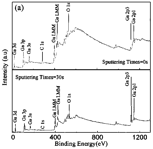
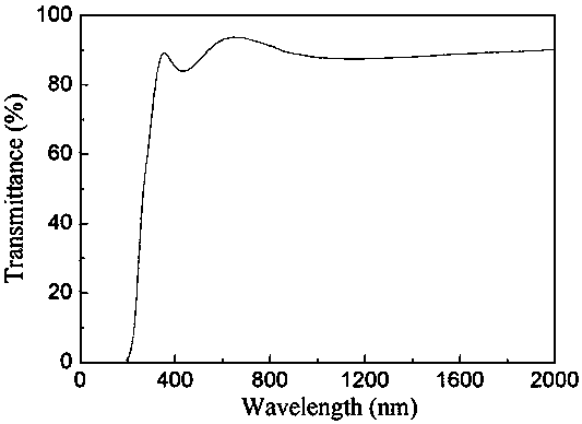
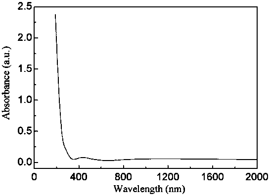
However, single crystal Ga 2 o 3 The preparation cost itself is high and it is not easy to obtain, so Ga 2 o 3 The preparation cost of the film; at the same time, a large amount of oxygen and a higher deposition temperature must be introduced during the metal evaporation Ga process to fully oxidize Ga to form Ga 2 o 3 Thin films, these conditions often put forward higher requirements for equipment capabilities, which increases the difficulty of the film preparation process, and insufficient oxidation will cause the film to have low transmittance and large absorption at around 350nm.

Method used


Image

  • Method for preparing Ga2O3 optoelectronic film by adopting electron beam evaporation technique
  • Method for preparing Ga2O3 optoelectronic film by adopting electron beam evaporation technique
  • Method for preparing Ga2O3 optoelectronic film by adopting electron beam evaporation technique

Examples


Embodiment 1

[0023] 1), with Ga 2 o 3 Powder (purity higher than 99.995%) is used as raw material, the powder is ground and granulated, and then cold-pressed into a cylindrical sample, and then cold isostatic pressed at 100MPa. o Pre-burning in C for 5 hours, and then in a vacuum of 1×10 -1 700 under Pa o C insulation 5h sintering.

[0024] 2) Crush the vacuum-sintered compact into irregular particles of 3-5 mm in size, and place it in a water-cooled crucible in the coating vacuum chamber, and pump the vacuum to 1×10 -3 Pa; while heating the substrate, the heating temperature is 25 o c.

[0025] 3) When the vacuum degree and heating temperature meet the set requirements, open the ventilation valve, and introduce high-purity oxygen (purity 99.999%) into the vacuum chamber, and the oxygen partial pressure is 1.4×10 -2 Pa, and maintain the corresponding vacuum for 5 minutes, and then start coating after stabilization.

[0026] 4) Close the baffle of the evaporation source, turn on the ...

Embodiment 2

[0030] 1) , with Ga 2 o 3 Powder (purity higher than 99.995%) is used as raw material, the powder is ground and granulated, and then cold-pressed into a cylindrical sample, and then cold isostatic pressed at 300MPa. o Pre-burn in C for 1 hour, and then in a vacuum of 1×10 -1 1200 under Pa o C insulation 1h sintering.

[0031] 2) Crush the vacuum sintered compact into irregular particles of 3-5 mm in size, and place them in a water-cooled crucible in the coating vacuum chamber, and pump the vacuum to 1.5×10 -3 Pa; while heating the substrate, the heating temperature is 25 o c.

[0032] 3) When both the vacuum degree and the heating temperature meet the set requirements, open the ventilation valve and introduce high-purity oxygen (purity 99.999%) into the vacuum chamber, and the oxygen partial pressure is 2.6×10 -2 Pa, and maintain the corresponding vacuum for 5 minutes, and then start coating after stabilization.

[0033] 4) Close the baffle of the evaporation source, tu...

Embodiment 3

[0037] 1), with Ga 2 o 3 Powder (purity higher than 99.995%) is used as raw material, the powder is ground and granulated, and then cold-pressed into a cylindrical sample, and then cold isostatic pressed at 150MPa. oPre-burning in C for 3 hours, and then in a vacuum of 5×10 -1 1000 under Pa o C insulation 3h sintering.

[0038] 2) Crush the vacuum-sintered compact into irregular particles of 3-5 mm in size, and place them in a water-cooled crucible in the coating vacuum chamber, and pump the vacuum to 4×10 -3 Pa; while heating the substrate, the heating temperature is 25 o c.

[0039] 3) When the vacuum degree and heating temperature meet the set requirements, open the ventilation valve and feed high-purity oxygen (purity 99.999%) into the vacuum chamber, and the oxygen partial pressure is 1.8×10 -2 Pa, and maintain the corresponding vacuum for 5 minutes, and then start coating after stabilization.

[0040] 4) Close the evaporation source baffle, turn on the electron gu...


PUM


Abstract

The invention belongs to the technical field of optoelectronic film preparation, and particularly relates to a method for preparing a Ga2O3 optoelectronic film by adopting an electron beam evaporationtechnique. The method adopts the technical scheme that Ga2O3 high-purity (99.995%) powder is prepared into blank and is sintered in a vacuum condition and then is crushed into granules as plating materials, direct vacuum evaporation is performed on the plating materials by adopting an e-shaped gun, so that the plating materials are gasified into molecules or atoms deposited on substrate materials, and finally, the large-area high-purity Ga2O3 film is obtained by controlling key technological parameters including the deposition rate, the deposition atmosphere and the like. The method has the advantages of low preparation cost, good repeatability, simple technological requirement and good controllability, the obtained film is of an isotropous amorphous structure, in a visible-near infraredrange, the transmittance is high, the absorption is low, and the film is suitable for optical application and has the characteristics of ultraviolet optoelectronic detection, gas sensing and the likeafter being crystallized through post annealing treatment.

Description

technical field [0001] The invention belongs to the technical field of photoelectric thin film preparation, in particular to a method for preparing Ga 2 o 3 method for photoelectric thin films. technical background [0002] Gallium oxide is a direct, wide-bandgap n-type semiconductor material with a forbidden band width of 4.9eV. It can prepare excellent deep-ultraviolet transparent conductive films. It has great potential in high-temperature oxidation sensors, ultraviolet detectors, and transparent electrodes of optoelectronic devices. Wide range of applications. Related research can be traced back to the 1960s. In recent years due to Ga 2 o 3 Thin film has the advantages of good light transmission from ultraviolet to near infrared, high refractive index and small absorption coefficient, and very good chemical stability, making it one of the optoelectronic materials that has attracted much attention at present. [0003] Currently, the preparation of Ga 2 o 3 There a...

Claims


Application Information

Patent Timeline
Patent Type & Authority Applications(China)
IPC IPC(8): C23C14/08C23C14/30
CPCC23C14/08C23C14/30
Inventor 杨陈张进蔡长龙徐均琪
Owner XIAN TECH UNIV
Learn More