
Material splitting manipulator for printed circuit boards (PCB) and processing system

A technology of PCB boards and manipulators, applied in the field of material distribution manipulators and processing systems, can solve the problems of increasing production processes, reducing production efficiency, and low degree of automation, and achieves the effect of ingenious structural design

Pending Publication Date: 2018-08-17
TIANJIN MEISEN ELECTRONICS CO LTD
View PDF0 Cites 0 Cited by
  • Summary
  • Abstract
  • Description
  • Claims
  • Application Information

AI Technical Summary

Problems solved by technology

On the one hand, since the substrate needs to be subjected to a certain cutting force when contact cutting is used, the clamping force on the substrate increases, which easily damages the tiny circuits in the board; on the other hand, high-pressure water cutting and mechanical tool cutting also It will cause water droplets and cutting powder on the substrate, which requires additional processing, which not only increases the production process, reduces production efficiency, but also increases production costs
In addition, the traditional PCB board cutting equipment, whether it is cutting with high-pressure water or grinding wheel, has a relatively low degree of automation. Affected by the cutting force, the positioning and clamping mechanism of the PCB board is easy to damage the circuit on the board, and the processing accuracy is not very good. high

Method used


Image

  • Material splitting manipulator for printed circuit boards (PCB) and processing system
  • Material splitting manipulator for printed circuit boards (PCB) and processing system
  • Material splitting manipulator for printed circuit boards (PCB) and processing system

Examples


Embodiment Construction

[0026] It should be noted that, in the case of no conflict, the embodiments of the present invention and the features in the embodiments can be combined with each other.

[0027] In describing the present invention, it should be understood that the terms "center", "longitudinal", "transverse", "upper", "lower", "front", "rear", "left", "right", The orientations or positional relationships indicated by "vertical", "horizontal", "top", "bottom", "inner", "outer", etc. are based on the orientation or positional relationships shown in the drawings, and are only for the convenience of describing the present invention Creation and simplification of description, rather than indicating or implying that the device or element referred to must have a specific orientation, be constructed and operate in a specific orientation, and therefore should not be construed as limiting the invention. In addition, the terms "first", "second", etc. are used for descriptive purposes only, and should no...


PUM


Abstract

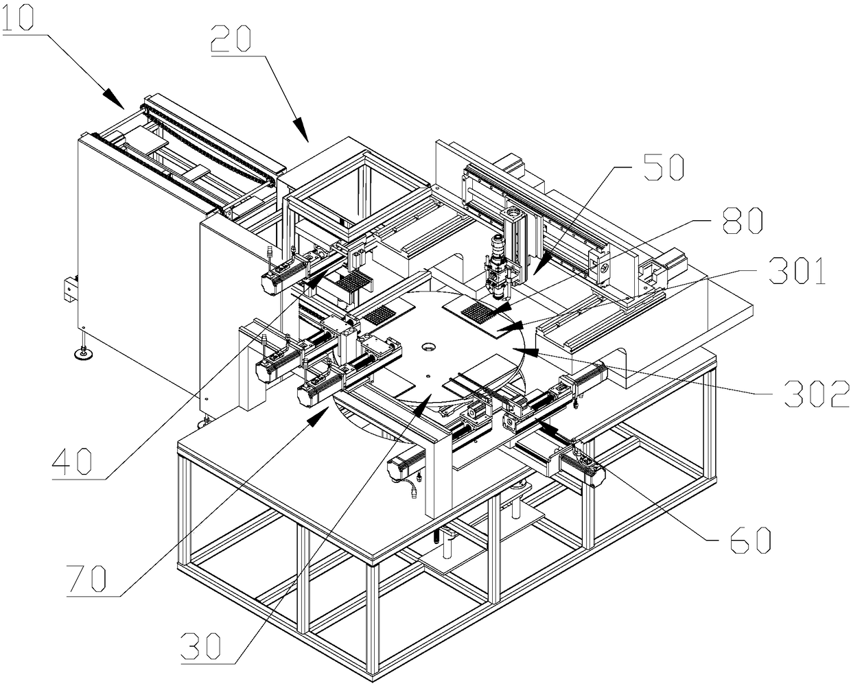
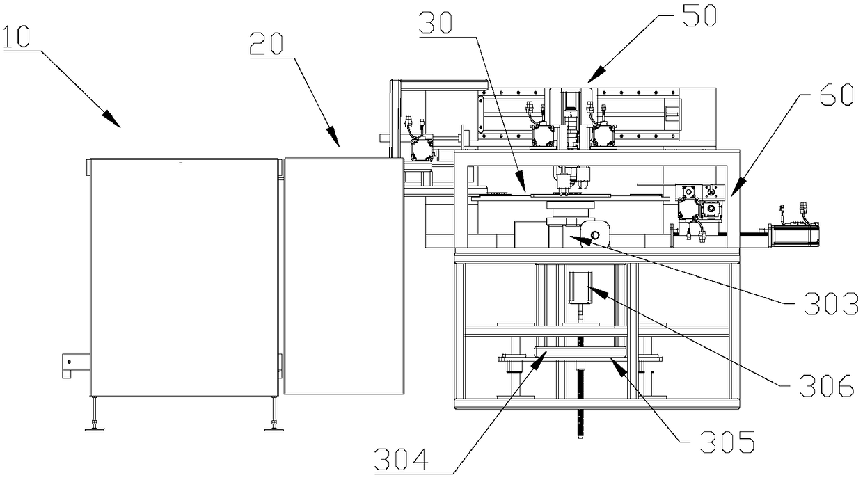
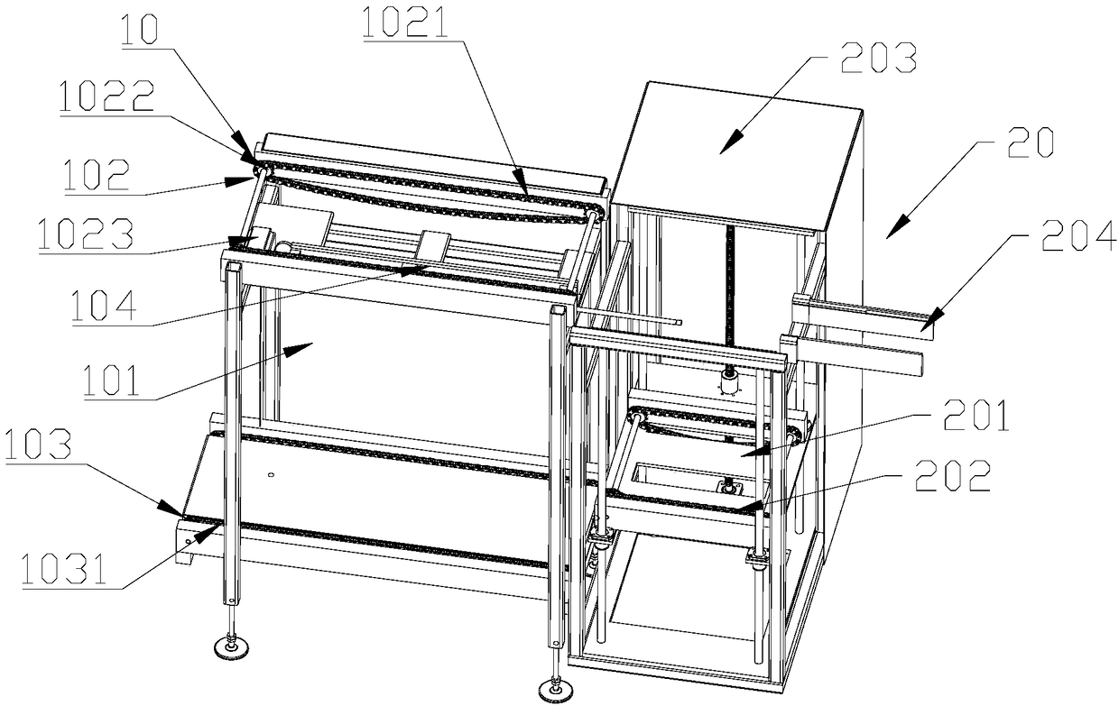
The invention provides a material splitting manipulator for printed circuit boards (PCB) and a processing system. The material splitting manipulator comprises a sliding table seat, wherein the slidingtable seat is arranged on one side of a rotating disk, the sliding table seat is arranged on a material splitting linear motor, the moving direction of the sliding table seat is the radial directionof the rotating disk, a material splitting cylinder is arranged on the sliding table seat, the material splitting cylinder is fixed to a material splitting translation device by virtue of a cylinder seat, the material splitting cylinder is driven to translate by the material splitting translation device, the translation direction of the material splitting cylinder is perpendicular to that of the sliding table seat, a telescopic rod of the material splitting cylinder is fixedly connected to one end of a movable material splitting finger, and one end of a fixed material splitting finger which corresponds to the movable material splitting finger is fixed to the cylinder seat. According to the material splitting manipulator, the cut PCBs are separated by the fixed material splitting finger andthe movable material splitting finger, so that the PCBs are convenient to grab by a subsequent material taking manipulator, and chips on the PCBs are effectively prevented from being damaged when thePCBs are grabbed.

Description

technical field [0001] The invention belongs to the technical field of PCB board cutting, and in particular relates to a laser PCB board distributing manipulator and a processing system. Background technique [0002] In the production and processing of electronic products, PCB boards are often used. The PCB board in the prior art is a whole traditional PCB board. The general cutting equipment of PCB boards uses contact means such as high-pressure water or mechanical tools (such as grinding wheels). Realize the cutting of the substrate. On the one hand, due to the need to subject the substrate to a certain cutting force when using contact cutting, the clamping force on the substrate will increase, which will easily damage the tiny circuits in the board; on the other hand, high-pressure water cutting and mechanical cutting It will cause water droplets and cutting powder on the substrate, which requires additional processes to be processed, which not only increases the product...

Claims


Application Information

Patent Timeline
IPC IPC(8): B24B27/06B24B41/00B24C1/04B24C9/00
CPCB24B27/06B24B41/005B24C1/045B24C9/00
Inventor 薛瑞华杨天伟李勇刚裴华磊
Owner TIANJIN MEISEN ELECTRONICS CO LTD
Learn More