Organic light emitting diode packaging structure and manufacturing method thereof as well as display device

A technology of light-emitting diodes and packaging structures, which is applied in semiconductor/solid-state device manufacturing, electrical components, electrical solid-state devices, etc., can solve problems such as increasing adhesion, achieve the goal of increasing adhesion, preventing packaging failure, and ensuring reliability Effect

Inactive Publication Date: 2018-08-14
WUHAN CHINA STAR OPTOELECTRONICS SEMICON DISPLAY TECH CO LTD
View PDF3 Cites 3 Cited by
  • Summary
  • Abstract
  • Description
  • Claims
  • Application Information

AI Technical Summary

Problems solved by technology

[0004] The present application provides an organic light-emitting diode packaging structure, its preparation method, and a display device, which can increase the adhesion between the organic layer and the inorganic layer, thereby preventing the display device from peeling off between the packaging layers during the bending or folding process, resulting in The problem of package failure, so as to ensure the reliability of flexible display devices

Method used


Image

  • Organic light emitting diode packaging structure and manufacturing method thereof as well as display device
  • Organic light emitting diode packaging structure and manufacturing method thereof as well as display device
  • Organic light emitting diode packaging structure and manufacturing method thereof as well as display device

Examples


Embodiment Construction

[0016] The following will clearly and completely describe the technical solutions in the embodiments of the present application in conjunction with the drawings in the embodiments of the present application. Obviously, the described embodiments are only a part of the embodiments of the present application, rather than all the embodiments. Based on the embodiments in this application, all other embodiments obtained by those of ordinary skill in the art without creative work fall within the protection scope of this application.

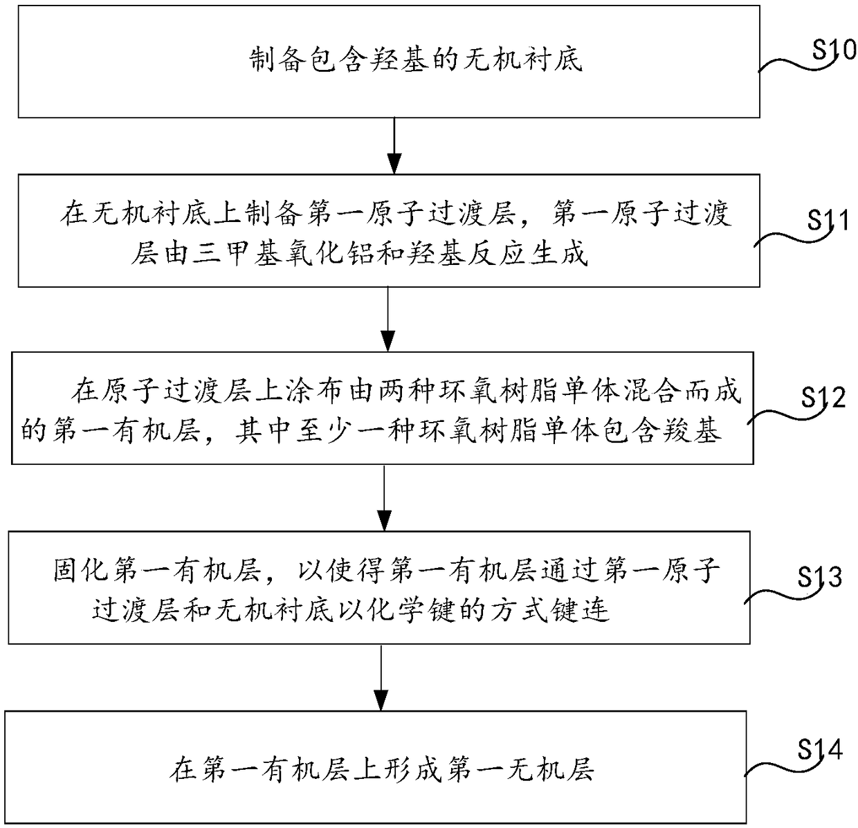
[0017] See figure 1 , figure 1 This is a schematic flow chart of the first embodiment of the manufacturing method of the organic light emitting diode packaging structure of this application. Such as figure 1 As shown, the specific preparation of the organic light emitting diode packaging structure in this application includes the following steps:

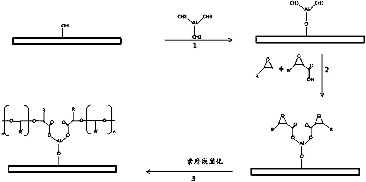
[0018] S10, preparing an inorganic substrate containing hydroxyl groups.

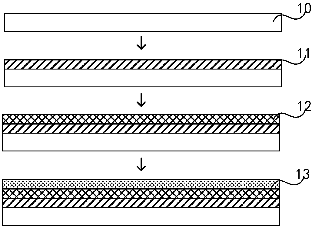
[0019] Please refer to figure 2 and ...


PUM


Abstract

The invention discloses an organic light emitting diode packaging structure and a manufacturing method thereof as well as a display device. The manufacturing method comprises the steps: manufacturingan inorganic substrate including hydroxyl; manufacturing a first atom transition layer on the inorganic substrate; coating a first organic layer, formed by mixing two epoxy resin monomers, on the atomtransition layer; and solidifying the first organic layer, so that the first organic layer is bonded with the inorganic substrate through the first atom transition layer in a chemical bond manner. Bythe above mode provided by the invention, the adhesiveness between the organic layer and the inorganic layer is increased, and a problem of package failure caused by packaging layer peeling in a display device bending or folding the procedure is avoided.

Description

Technical field [0001] This application relates to the field of display technology, in particular to an organic light emitting diode packaging structure and a display device. Background technique [0002] Organic light-emitting diodes (Organic Light-Emitting Diode, OLED), as a new generation of display technology, have received widespread attention because they can be made thinner and can achieve flexible displays. At present, one of the important factors restricting flexible display is the packaging technology. OLED uses small or large molecules to apply voltage through the anode and cathode to form electroluminescence. These luminescent materials are easily cracked in the presence of water or oxygen, thereby affecting The lifespan of OLEDs therefore puts forward higher requirements for OLED packaging. [0003] Thin-film packaging technology is currently the most widely studied packaging technology for flexible displays. It generally uses an inorganic / organic alternating structur...

Claims


Application Information

Patent Timeline
Patent Type & Authority Applications(China)
IPC IPC(8): H01L51/52H01L51/56
CPCH10K50/844H10K2102/311H10K71/00
Inventor 金江江徐湘伦
Owner WUHAN CHINA STAR OPTOELECTRONICS SEMICON DISPLAY TECH CO LTD
Why Eureka
Try Eureka