Ultrasonic atomization pyrolytic deposition device and method for preparing thin film by using device
An ultrasonic atomization and deposition device technology, applied in gaseous chemical plating, metal material coating process, coating, etc., can solve the problems of unstable film formation, small film formation area, poor film formation uniformity, etc., and achieve the goal of manufacturing The effect of short cycle, low price, optimization of gas diffusion direction and uniformity
- Summary
- Abstract
- Description
- Claims
- Application Information
AI Technical Summary
Problems solved by technology
Method used
Image
Examples
Embodiment 1
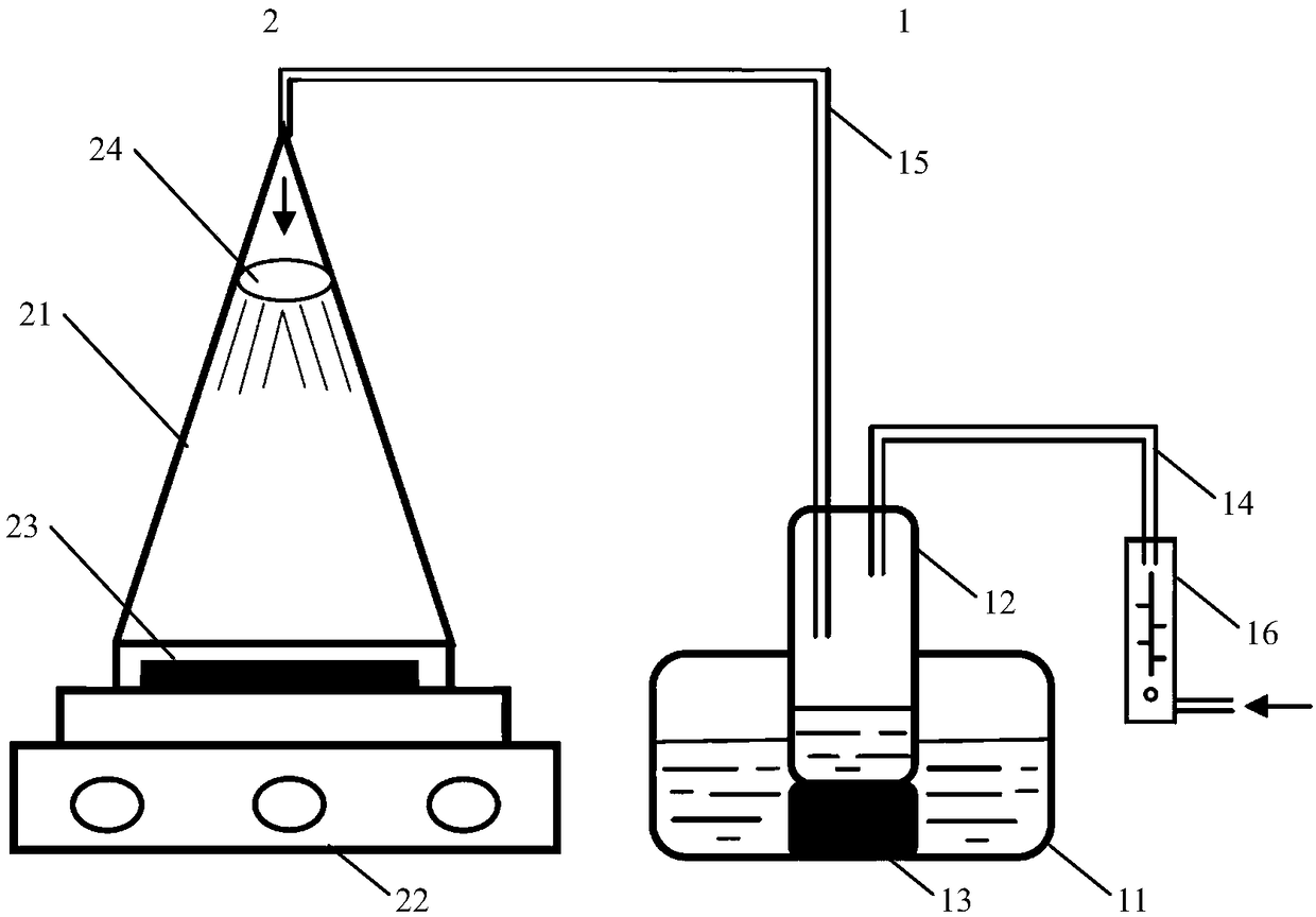
[0058] Cleaning the film growth substrate: Clean the surface of the film growth substrate with surfactant, rinse with deionized water, dry the surface with an air gun, dry in an oven or immerse the film growth substrate in acetone solution, ultrasonically clean, and dry the surface with an air gun , into the oven to dry. Place the cleaned thin film growth substrate at the bottom of the conical growth chamber. The film growth substrate used is a circular glass substrate with a diameter of 22 cm and an area of 380 cm 2 .
[0059] Atomization: Take an appropriate amount of solution and pour it into the atomization bottle. In order to ensure the amount of atomization, avoid pouring too much solution. Thin film growth precursor solution is added in atomizing bottle, used thin film growth precursor solution is formulated by weak acid salt (for example, can select acetate for use) and catalyst solution, and used catalyst solution is the weak alkali solution that pH is 7.2, The p...
Embodiment 2
[0065] Preparation method is basically the same as Example 1, except that:
[0066] Set the carrier gas flow rate to 5L / min;
[0067] The thin film growth substrate was heated to 320°C.
[0068] The prepared product is a transparent film with high crystalline quality and visible light transmittance.
[0069] Film area up to 376cm 2 , accounting for 99% of the film growth substrate area.
[0070] Measure the thickness somewhere on the edge of the film and compare it with the thickness somewhere in the middle of the film. The difference between the former and the latter is only -0.021mm.
Embodiment 3
[0072] Preparation method is basically the same as Example 1, except that:
[0073] Set the carrier gas flow rate to 6L / min;
[0074] The thin film growth substrate was heated to 350°C.
[0075] The prepared product is a transparent film with high crystalline quality and visible light transmittance.
[0076] Film area up to 375cm 2 , accounting for 99% of the film growth substrate area.
[0077] Measure the thickness somewhere on the edge of the film and compare it with the thickness somewhere in the middle of the film. The difference between the former and the latter is only -0.019mm.
PUM
 Abstract
Description
Claims
Application Information
 - R&D
- Intellectual Property
- Life Sciences
- Materials
- Tech Scout
- Unparalleled Data Quality
- Higher Quality Content
- 60% Fewer Hallucinations
Browse by: Latest US Patents, China's latest patents, Technical Efficacy Thesaurus, Application Domain, Technology Topic, Popular Technical Reports.
© 2025 PatSnap. All rights reserved.Legal|Privacy policy|Modern Slavery Act Transparency Statement|Sitemap|About US| Contact US: help@patsnap.com


