Monocrystalline semiconductor wafer and method for producing semiconductor wafer

A single crystal semiconductor, semiconductor technology, applied in semiconductor devices, semiconductor/solid-state device manufacturing, semiconductor/solid-state device testing/measurement, etc., can solve problems such as inability to achieve flatness, inability to achieve long-wavelength roughness, etc.

Active Publication Date: 2018-08-03
SILTRONIC AG
View PDF10 Cites 2 Cited by
  • Summary
  • Abstract
  • Description
  • Claims
  • Application Information

AI Technical Summary

Problems solved by technology

This in turn is associated with an inevitable deterioration of the flatness in the outermost edge region of the wafer, so that even with the aid of PACE an arbitrarily good flatness in the edge region cannot be achieved
Furthermore, fog-free polishing, usually performed as single-sided polishing, cannot in principle achieve good leveling of long-wavelength roughness (e.g., with a cut-off wavelength of 250 microns), especially if a soft fog-free polishing pad is used

Method used


Image

  • Monocrystalline semiconductor wafer and method for producing semiconductor wafer
  • Monocrystalline semiconductor wafer and method for producing semiconductor wafer

Examples


Embodiment Construction

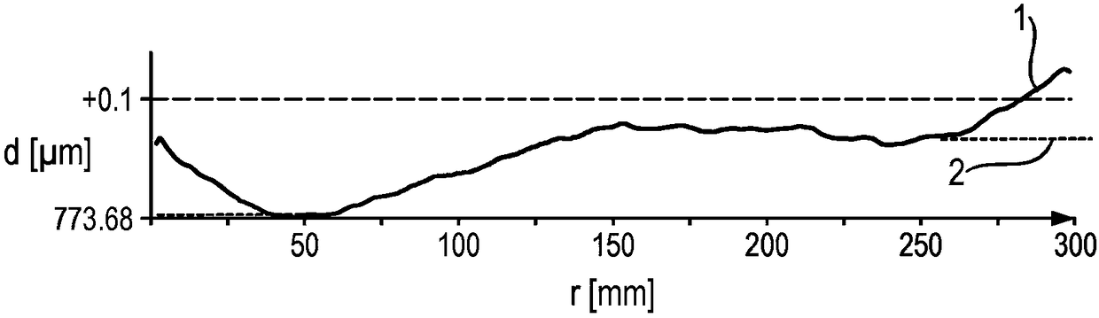
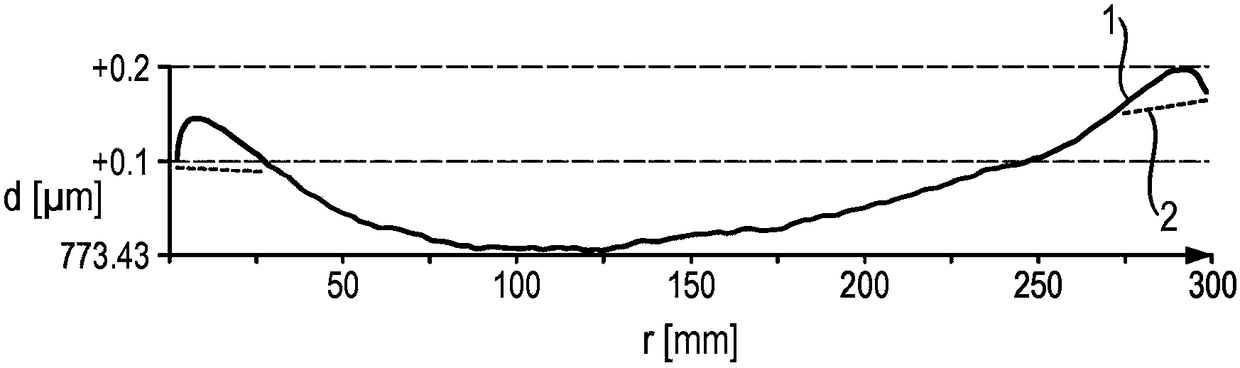
[0021] The semiconductor wafer according to the invention is characterized by a roughness R of 0.8 nm or less, preferably 0.5 nm or less a ("average roughness"), which is typical of polished semiconductor wafers. The stated values ​​relate to the average roughness determined by white light interferometry at a cut-off wavelength of 250 μm. At the same time, however, the semiconductor wafer according to the invention has a value ESFQR of 8 nm or less, preferably 5 nm or less avg - characterizes the flatness in the edge region. Roughness R as low as 0.2 nm or even 0.1 nm can be achieved by means of fog-free polishing according to the state of the art a .

[0022] The semiconductor wafers according to the invention are thus much less rough than after PACE processing and, on the other hand, are significantly flatter at the edges than after double-sided and single-sided polishing according to the prior art.

[0023] Preferably, the semiconductor wafer according to the invention ...


PUM


Abstract

The invention relates to a monocrystalline semiconductor wafer having an average roughness Ra of at most 0.8 nm at a cut-off wavelength of 250 [mu]m. The wafer is characterized by an ESFQRavg of 8 nmor less at an edge exclusion of 1 mm. The invention further relates to a method for producing a monocrystalline semiconductor wafer. The method comprises the following steps in the specified order: polishing the semiconductor wafer on both sides simultaneously; locally processing at least part of at least one side of the semiconductor wafer in a material-removing manner by means of a liquid jet, which contains suspended hard-material particles and which is directed at a small area of the surface by means of a nozzle, wherein the nozzle is moved over the part of the surface to be treated in such a way that a predefined geometry parameter of the semiconductor wafer is improved; and polishing the at least one surface of the semiconductor wafer.

Description

technical field [0001] The invention relates to a monocrystalline semiconductor wafer having a low roughness R in the region adjacent to the edge a and outstanding flatness. The invention also relates to a multi-step method suitable for producing such semiconductor wafers. Background technique [0002] Monocrystalline semiconductor wafers, such as silicon wafers, for the production of electronic components must have extremely flat surfaces. Otherwise, structures in the nanometer range cannot be clearly imaged on the surface during photolithography. Due to the miniaturization of electronic devices that is being further advanced, requirements regarding flatness are continuously increasing. In this case, the region of the silicon wafer immediately adjacent to the edge is particularly difficult to planar due to various influences. Double-sided polishing is a suitable method for obtaining extremely flat silicon wafers with good local geometry values ​​in the edge region in se...

Claims


Application Information

Patent Timeline
Patent Type & Authority Applications(China)
IPC IPC(8): H01L21/02H01L21/304H01L21/66
CPCH01L22/12H01L22/20H01L21/3046H01L21/02021H01L21/02024H01L21/02598H01L21/02013H01L21/02016H01L21/02019H01L21/02052H01L21/30625H01L21/67051H01L29/16
Inventor K·勒特格H·贝克尔L·米斯图尔A·米厄
Owner SILTRONIC AG
Why Eureka
Try Eureka