Back face passivated laser slotted solar cell and manufacturing method thereof
A technology of backside passivation and laser grooving, which is applied in the direction of photovoltaic power generation, circuits, electrical components, etc., can solve the problems of large stress on crystalline silicon wafers, limited collection dimensions, and large active area, so as to reduce debris and enhance collection ability, the effect of reducing the conduction resistance
- Summary
- Abstract
- Description
- Claims
- Application Information
AI Technical Summary
Problems solved by technology
Method used
Image

Examples
Embodiment 1
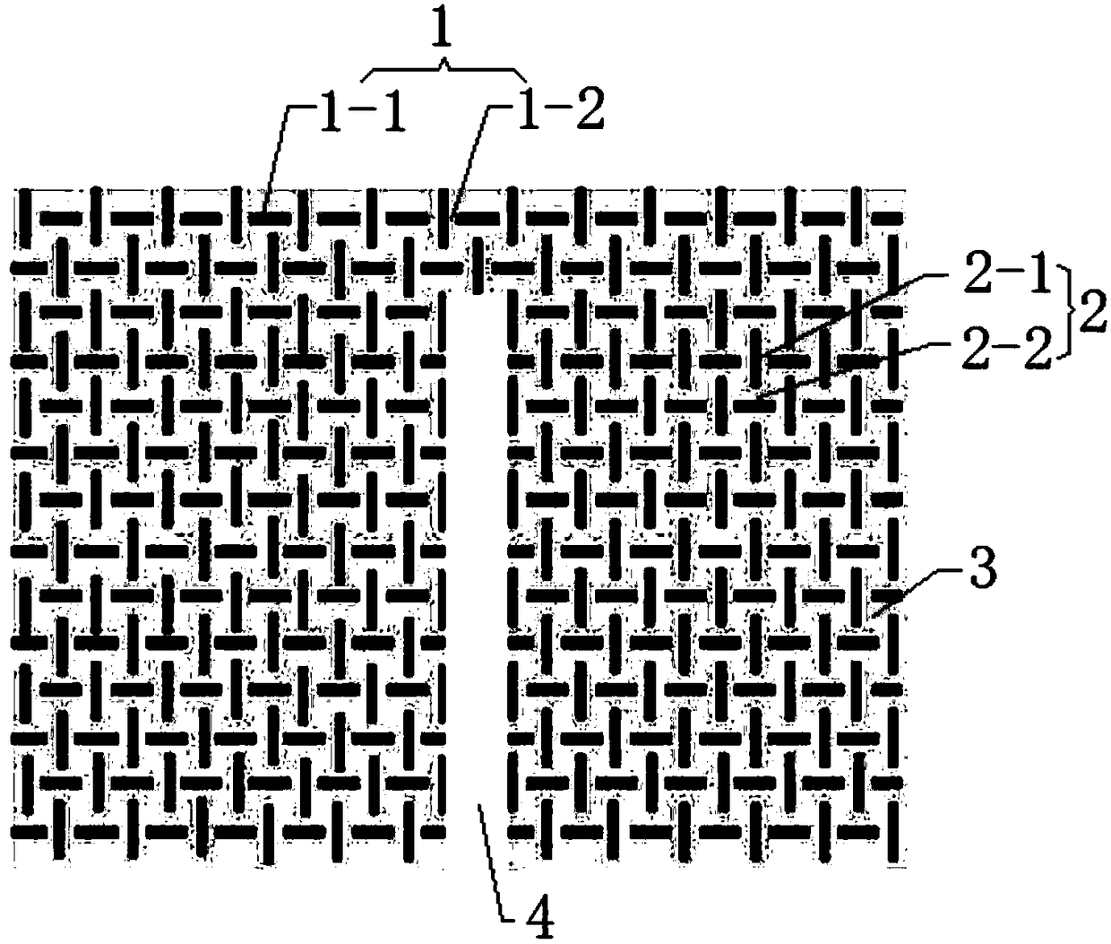
[0052] Such as figure 1 As shown, the present embodiment provides a back passivation laser grooved solar cell, comprising a solar grade crystalline silicon wafer provided with a back passivation film 3, on which a number of parallel arrays are evenly arranged on the back passivation film 3 Spacer lines 1 and several vertically arranged spacer lines 2 vertically intersecting with several parallel spacer lines 1, in this embodiment, a laser spot with a certain wavelength and a suitable size is used for slotting on the passivation film 3 on the back of the crystalline silicon wafer. The back passivation film 3 includes but not limited to aluminum oxide, silicon oxide, silicon dioxide, silicon oxynitride, silicon carbide and stacks of different combinations thereof. The thickness of the stacked film is 150nm. Square spot, the laser spot size on the laminated film is 35um, the Ag / Ag-Al electrode 4 and the epitaxial 0.8mm area on the back of the battery are not laser grooved, which ...
Embodiment 2
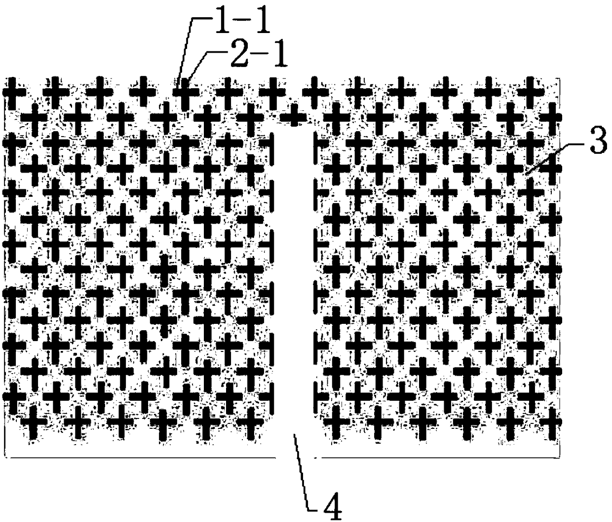
[0077] Such as figure 2 As shown, the present embodiment provides a back passivation laser grooved solar cell, comprising a solar grade crystalline silicon wafer provided with a back passivation film 3, on which a number of parallel arrays are evenly arranged on the back passivation film 3 Spacer lines 1 and several vertically arranged spacer lines 2 vertically intersecting with several parallel spacer lines 1, in this embodiment, a laser spot with a certain wavelength and a suitable size is used for slotting on the passivation film on the back of the crystalline silicon wafer. The back passivation film includes but not limited to aluminum oxide, silicon oxide, silicon dioxide, silicon oxynitride, silicon carbide and their different combinations. The thickness of the laminated film is 183nm. The laser spot adopts a square spot with a wavelength of 1064nm , the laser spot size on the laminated film is 45um, no laser slots are used on the back of the battery to lead out the Ag / ...
Embodiment 3
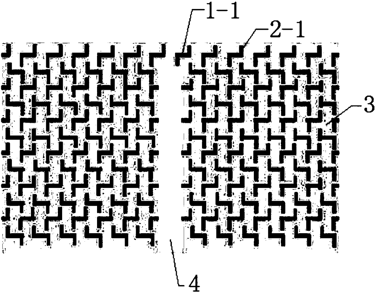
[0101] Such as image 3 As shown, the present embodiment provides a back passivation laser grooved solar cell, comprising a solar grade crystalline silicon wafer provided with a back passivation film 3, on which a number of parallel arrays are evenly arranged on the back passivation film 3 Spacer lines 1 and several vertically arranged spacer lines 2 vertically intersecting with several parallel spacer lines 1, in this embodiment, a laser spot with a certain wavelength and a suitable size is used for slotting on the passivation film on the back of the crystalline silicon wafer. The rear passivation film includes but is not limited to aluminum oxide, silicon oxide, silicon dioxide, silicon oxynitride, silicon carbide and their different combinations. The thickness of the laminated film is 150nm. Spot, the laser spot size on the laminated film is 60um, no laser slots are used on the back of the battery to lead out the Ag / Ag-Al electrode 4 and the area of the epitaxial 0.2mm, w...
PUM
 Abstract
Description
Claims
Application Information
 - R&D
- Intellectual Property
- Life Sciences
- Materials
- Tech Scout
- Unparalleled Data Quality
- Higher Quality Content
- 60% Fewer Hallucinations
Browse by: Latest US Patents, China's latest patents, Technical Efficacy Thesaurus, Application Domain, Technology Topic, Popular Technical Reports.
© 2025 PatSnap. All rights reserved.Legal|Privacy policy|Modern Slavery Act Transparency Statement|Sitemap|About US| Contact US: help@patsnap.com