ESD (electrostatic discharge) device structure

An ESD device and asymmetric structure technology, applied in the semiconductor field, can solve problems such as large latchup risk

Active Publication Date: 2018-07-13
SHANGHAI HUAHONG GRACE SEMICON MFG CORP
View PDF4 Cites 6 Cited by
  • Summary
  • Abstract
  • Description
  • Claims
  • Application Information

AI Technical Summary

Problems solved by technology

However, the maintenance voltage Vh of the pure SCR structure after snapback generally does not exceed 10V, and there is a greater risk of latchup in the application of high-voltage ports.

Method used


Image

  • ESD (electrostatic discharge) device structure
  • ESD (electrostatic discharge) device structure
  • ESD (electrostatic discharge) device structure

Examples


Embodiment Construction

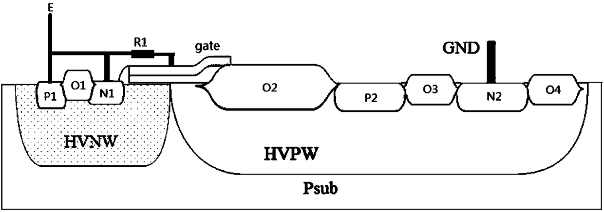
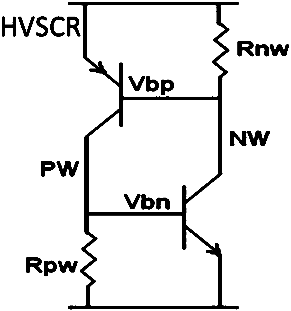
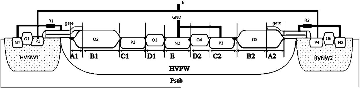
[0043] The ESD device structure of the present invention includes: a first LDMOS, a second LDMOS and a parasitic SCR;

[0044] The first PLDMOS and the second LDMOS are P-LDMOS with the same structure and layout sharing a high-voltage P well (HVPW), and the high-voltage P well (HVPW) between the first P-LDMOS drain and the second P-LDMOS drain The parasitic SCR formed by the N+ region is arranged in the middle, and the first P-LDMOS and the second P-LDMOS form a left-right asymmetric structure centering on the N+ region of the parasitic SCR. The width (A1+B1) of the field oxygen region between the first LDMOS gate and the drain is greater than the width (A2+B2) of the field oxygen region between the second LDMOS gate and the drain, so that the structure can be reduced Turn on the voltage.

[0045] like image 3 As shown, a specific embodiment of the ESD of the present invention includes: a P-type substrate Psub, a first high-voltage N well HVNW1, a second high-voltage N well...


PUM


Abstract

The invention discloses an ESD (electrostatic discharge) device structure, comprising: a first P-LDMOS (P-type laterally diffused metal oxide semiconductor), a second P-LDMOS and a parasitic SCR (silicon controlled rectifier). The first P-LDMOS and the second P-LDMOS share a high-voltage P well (HVPW); an N+ AREA is arranged in the high-voltage P well (HVPW) between a drain of the first P-LDMOS and a drain of the second P-LDMOS to form the parasitic SCR; the first parasitic SCR and the second parasitic SCR have identical structure and are of bilateral asymmetric structure by centering on the N+ area. The ESD device structure has the advantages that ESD capacity of a device after being turned on can be improved, maintaining voltage and current can also be increased for the device, and latch-up risk of the ESD device is reduced.

Description

technical field [0001] The invention relates to the field of semiconductors, in particular to an ESD device structure. Background technique [0002] Static electricity is an objective natural phenomenon, which can be produced in many ways, such as contact, friction, induction between electrical appliances, etc. Static electricity is characterized by long-term accumulation, high voltage, low power, small current and short action time. Static electricity poses serious hazards in at least two areas. Friction electrification and human body static electricity are two major hazards in the electronics industry, which often cause unstable operation or even damage of electronic and electrical products. ESD is a discipline formed since the middle of the 20th century to study the generation, harm and protection of static electricity. It is customary in the world to refer to the equipment used for electrostatic protection as ESD. [0003] Conventional high-voltage ESD devices general...

Claims


Application Information

Patent Timeline
Patent Type & Authority Applications(China)
IPC IPC(8): H01L27/02
CPCH01L27/0266
Inventor 邓樟鹏苏庆韦敏侠
Owner SHANGHAI HUAHONG GRACE SEMICON MFG CORP
Why Eureka
Try Eureka