


Quick Research
Generate reliable direction feasibility study reports for your R&D in just a few steps.

Technical Q&A
Discover and master advanced knowledge NOW. Basics, ideas, possibilities, all at once.

Find Solutions
As an expert in R&D theories, this can generate solutions to your technical problems instantly.

Evaluate Feasibility
Analyze your overall solution with one click, know your potential R&D risks in advance.

Monitor Landscape
Get weekly tech updates, stay abreast of the latest tech innovations and key insights.
esd device structure
An ESD device, P-LDMOS technology, applied in the direction of semiconductor devices, electrical solid state devices, electrical components, etc., can solve problems such as large latchup risk
- Summary
- Abstract
- Description
- Claims
- Application Information
AI Technical Summary
Problems solved by technology
Method used
Image


Examples
Embodiment Construction
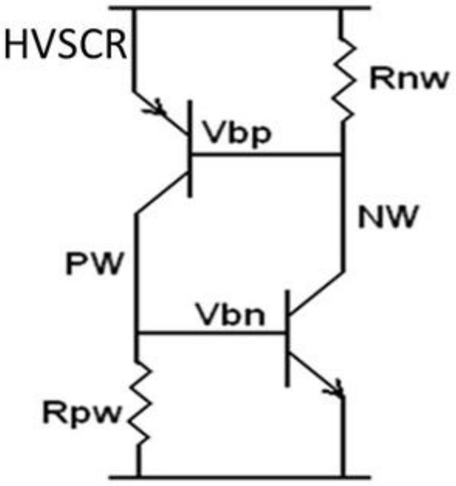
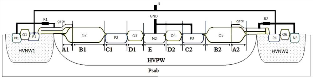
[0043] The ESD device structure of the present invention includes: a first LDMOS, a second LDMOS and a parasitic SCR;
[0044] The first PLDMOS and the second LDMOS are P-LDMOS with the same structure and layout sharing a high-voltage P-well (HVPW), and the high-voltage P-well (HVPW) between the drain of the first P-LDMOS and the drain of the second P-LDMOS The parasitic SCR formed by the N+ region is arranged in the middle, and the first P-LDMOS and the second P-LDMOS form a left-right asymmetric structure centering on the N+ region of the parasitic SCR. The width (A1+B1) of the field oxygen region between the gate and drain of the first LDMOS is greater than the width (A2+B2) of the field oxygen region between the gate and drain of the second LDMOS, so that the structure can be reduced Turn on the voltage.
[0045] Such as image 3 As shown, a specific embodiment of the ESD of the present invention includes: P-type substrate Psub, the first high-voltage N well HVNW1, the s...
PUM
 Abstract
Description
Claims
Application Information
 - R&D Engineer
- R&D Manager
- IP Professional
- Industry Leading Data Capabilities
- Powerful AI technology
- Patent DNA Extraction
Browse by: Latest US Patents, China's latest patents, Technical Efficacy Thesaurus, Application Domain, Technology Topic, Popular Technical Reports.
© 2024 PatSnap. All rights reserved.Legal|Privacy policy|Modern Slavery Act Transparency Statement|Sitemap|About US| Contact US: help@patsnap.com