Performance-adjustable high-stability resistive random access memory
A technology of resistive memory and stability, applied in electrical components and other directions, can solve the problems of unstable performance of resistive memory, misreading, miswriting, affecting data reliability, etc., to achieve easy operation, improve stability, and preparation process. simple effect
- Summary
- Abstract
- Description
- Claims
- Application Information
AI Technical Summary
Problems solved by technology
Method used
Image
Examples
Embodiment 1
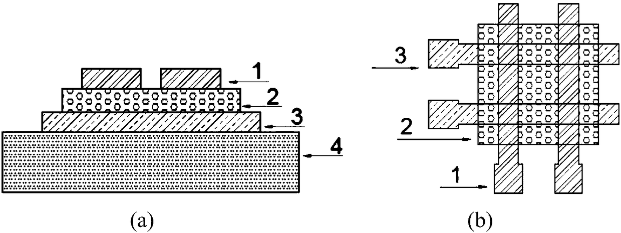
[0031] In the resistive variable memory prepared in this embodiment, the conductive oxide film is an ITO film with a thickness of 60 nm, and is placed between the bottom electrode and the resistive variable layer.
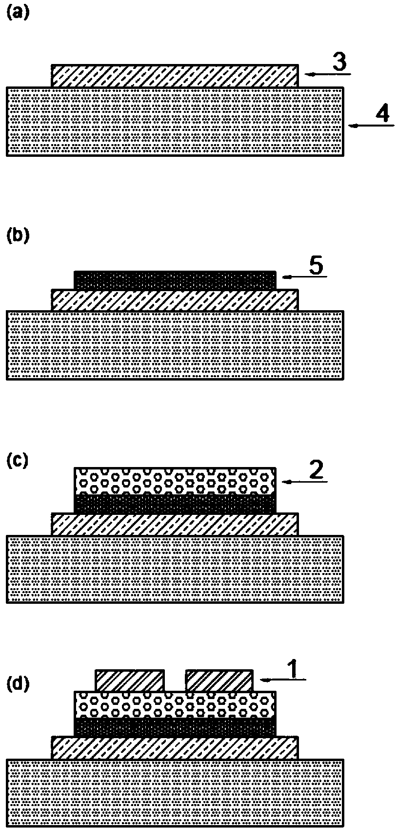
[0032] The specific preparation process is as figure 2 Shown:
[0033] First, an Al conductive film is deposited on the glass substrate 4, and the Al conductive film is etched to form a bottom electrode 3, such as figure 2 as shown in (a);
[0034] Then, deposit a thickness of 60nm ITO thin film on the bottom electrode 3 to form a performance control layer 5, such as figure 2 as shown in (b);
[0035] Next, deposit Al with a thickness of 10 nm on the performance regulation layer 5 2 o 3 film to form a resistive switch layer 2, such as figure 2 as shown in (c);
[0036] Finally, an Al conductive film is deposited on the resistive switch layer 2 to form a top electrode 1, such as figure 2 As shown in (d), the RRAM is obtained.
[0037] The resistive mem...
Embodiment 2
[0039] The process and parameters for preparing the resistive memory in this example are the same as those in Example 1, the difference is that in the resistive memory prepared in this example, an ITO film with a thickness of 60 nm is placed between the top electrode and the resistive layer. like Figure 4 shown.
[0040] The resistive memory prepared in this embodiment is tested, and the test results are: the activation voltage of the resistive memory is about 4V, the variation range of the set voltage is 0.2V, and the resistance ratio of the resistive memory is about 600-700.
Embodiment 3
[0042] The process and parameters for preparing the resistive memory in this example are the same as those in Example 1. The difference is that in the resistive memory prepared in this example, an ITO film with a thickness of 30 nm is placed between the bottom electrode and the resistive layer at the same time. and between the top electrode and the resistive layer, such as Figure 5 shown.
[0043] The resistive memory prepared in this embodiment is tested, and the test results are: the activation voltage of the resistive memory is about 4V, the variation range of the set voltage is 0.2V, and the resistance ratio of the resistive memory is about 600-700.
PUM
| Property | Measurement | Unit |
|---|---|---|
| Thickness | aaaaa | aaaaa |
| Thickness | aaaaa | aaaaa |
| Thickness | aaaaa | aaaaa |
Abstract
Description
Claims
Application Information
 - R&D Engineer
- R&D Manager
- IP Professional
- Industry Leading Data Capabilities
- Powerful AI technology
- Patent DNA Extraction
Browse by: Latest US Patents, China's latest patents, Technical Efficacy Thesaurus, Application Domain, Technology Topic, Popular Technical Reports.
© 2024 PatSnap. All rights reserved.Legal|Privacy policy|Modern Slavery Act Transparency Statement|Sitemap|About US| Contact US: help@patsnap.com


