Ink-jet technology based LED display screen integrative mask
A technology of LED display and display screen, applied in the direction of instruments, identification devices, etc., can solve the problems that the authenticity of color difference cannot meet the requirements of the client, the channeling light and the color difference of the module do not have a good elimination method, etc., to solve the problem of patchwork And chromatic aberration problem, reduce chromatic aberration problem, solve the effect of channeling light
- Summary
- Abstract
- Description
- Claims
- Application Information
AI Technical Summary
Problems solved by technology
Method used
Image
Examples
Embodiment 1
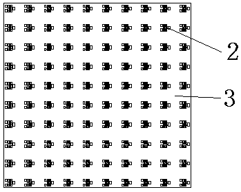
[0020] figure 1 The COB module packaging structure implemented by the existing technology does not have a virtual mask of the ink layer, and there is no good way to eliminate the color difference of the light channeling and the module, resulting in the fact that the color difference cannot meet the client's requirements.
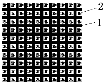
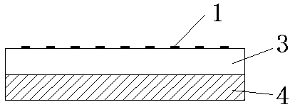
[0021] To optimize existing technologies such as figure 2 and image 3 As shown, the PCB substrate 4 with IC is solidified and wire bonded; the PCB substrate 4 after wire bonding is molded and sealed; the surface of the adhesive layer of the packaging adhesive 3 is subjected to patterned inkjet treatment and ink semi-curing, An integrated mask is formed between the pixel units 2 of the COB display screen; and then the ink is baked and solidified.
[0022] On the surface of the COB module, jet printing technology is used to realize "well" jet printing, so that the virtual mask 1 of "well" is realized between the single pixel units 2. The distance between ...
Embodiment 2
[0026] This embodiment is similar to Embodiment 1, the difference is that, as Figure 4 and Figure 5 As shown, on the surface of the COB module, the jet printing technology is used to realize the "well"-shaped jet printing, so that the "well"-shaped virtual mask 1 is realized between the 2*2 pixel units 2 . There are 4 pixel units 2 in the virtual mask 1 of the well, while Embodiment 1 is a single pixel unit 2, which can be printed according to the actual demand effect and the spacing of the pixel units 2.
PUM
 Abstract
Description
Claims
Application Information
 - R&D
- Intellectual Property
- Life Sciences
- Materials
- Tech Scout
- Unparalleled Data Quality
- Higher Quality Content
- 60% Fewer Hallucinations
Browse by: Latest US Patents, China's latest patents, Technical Efficacy Thesaurus, Application Domain, Technology Topic, Popular Technical Reports.
© 2025 PatSnap. All rights reserved.Legal|Privacy policy|Modern Slavery Act Transparency Statement|Sitemap|About US| Contact US: help@patsnap.com


