Substrate handling equipment and heat shields
A substrate processing device and heat shield technology, which is applied to discharge tubes, electrical components, circuits, etc., can solve problems such as increased radiated heat, and achieve the effect of preventing heat accumulation
Active Publication Date: 2019-12-24
TOKYO ELECTRON LTD
View PDF6 Cites 0 Cited by
- Summary
- Abstract
- Description
- Claims
- Application Information
AI Technical Summary
Problems solved by technology
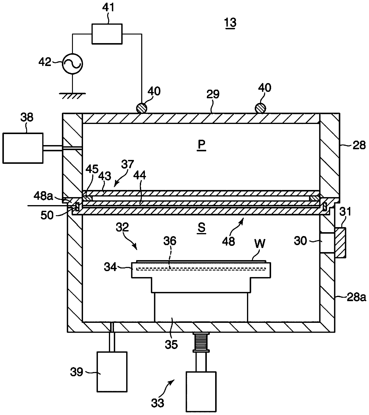
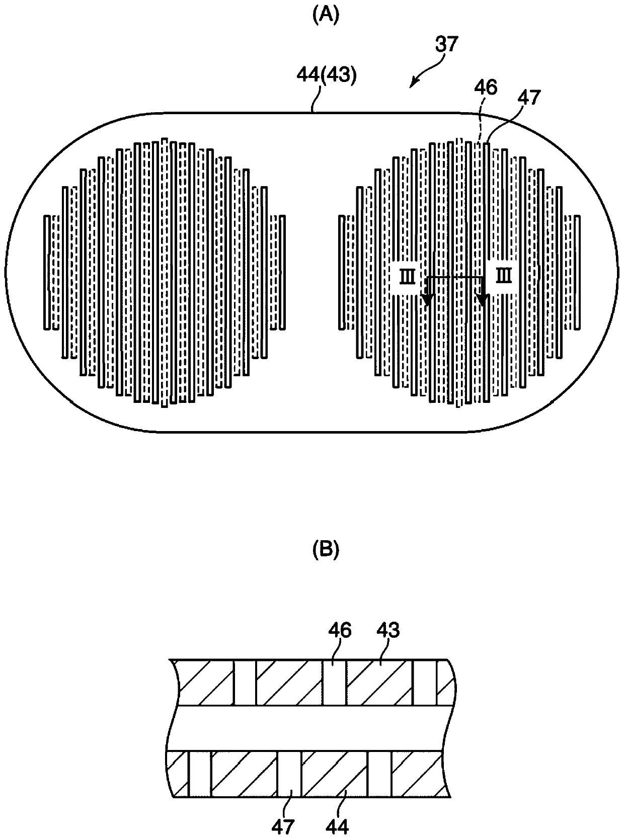
Therefore, in the ion trap facing the plasma, there are many ions colliding with the central part. If chemical etching treatment is repeated, for example, a lot of heat is accumulated in the central part of the ion trap. The central part of the collector faces the process space, and the radiant heat of the wafer increases
Method used
View moreImage
Smart ImageViewing Examples

Examples
Embodiment
[0062] Next, examples of the present invention will be described.
Login to View More PUM
 Abstract
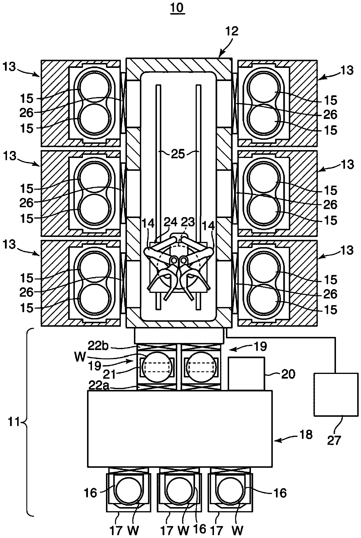
The invention provides a substrate processing device and a heat shield. The substrate processing apparatus can uniformly perform processing using radicals on a substrate even when processing is repeated. The process module (13) has: a processing container (28) for accommodating the wafer (W); (W); a heat shield (48), which is configured between the partition plate (37) and the wafer (W), and the partition plate (37) is selectively placed in the plasma generation space (P) Radicals in the generated plasma permeate toward the wafer (W), and the heat shield (48) is arranged in a manner facing the wafer (W). )connect.
Description
technical field [0001] The present invention relates to a substrate processing apparatus that processes a substrate using radicals in plasma, and a heat shield suitable for the substrate processing apparatus. Background technique [0002] In recent years, it has been proposed to chemically etch a semiconductor wafer (hereinafter simply referred to as “wafer”) as a substrate using radicals in plasma (see, for example, Patent Document 1). [0003] Such an apparatus for performing chemical etching treatment includes a plate-shaped ion trap that is interposed between the plasma and the wafer in the processing chamber, and controls the movement of ions in the plasma toward the wafer. inhibition. The ion trap has many slits penetrating in the thickness direction, blocks the movement of ions moving anisotropically, and transmits radicals moving isotropically through the labyrinth of the plurality of slits. As a result, almost only free radicals exist in the processing space facin...
Claims
Login to View More Application Information
Patent Timeline
 Patent Type & Authority Patents(China)
IPC IPC(8): H01J37/32
CPCH01J37/32522H01L21/31116H01L21/67103H01L21/6719H01J37/321H01J37/32357H01J37/32422H01J2237/334H01L21/67069H01L21/6835H01J2237/3174H01L21/3065
Inventor 小川裕之清水昭贵土场重树
Owner TOKYO ELECTRON LTD
Features
- R&D
- Intellectual Property
- Life Sciences
- Materials
- Tech Scout
- Unparalleled Data Quality
- Higher Quality Content
- 60% Fewer Hallucinations
Learn More Browse by: Latest US Patents, China's latest patents, Technical Efficacy Thesaurus, Application Domain, Technology Topic, Popular Technical Reports.
© 2025 PatSnap. All rights reserved.Legal|Privacy policy|Modern Slavery Act Transparency Statement|Sitemap|About US| Contact US: help@patsnap.com