A kind of organic light-emitting diode substrate and its preparation method, display panel
A technology of light-emitting diodes and substrates, applied in semiconductor devices, electrical components, circuits, etc., can solve problems such as poor uniformity of film morphology, achieve balanced redistribution process, slow down solvent evaporation, improve life and display effects
- Summary
- Abstract
- Description
- Claims
- Application Information
AI Technical Summary
Problems solved by technology
Method used
Image

Examples
no. 1 example
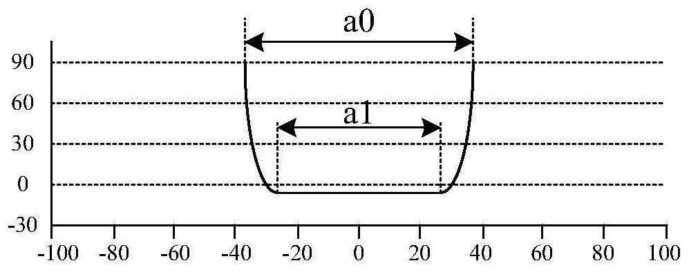
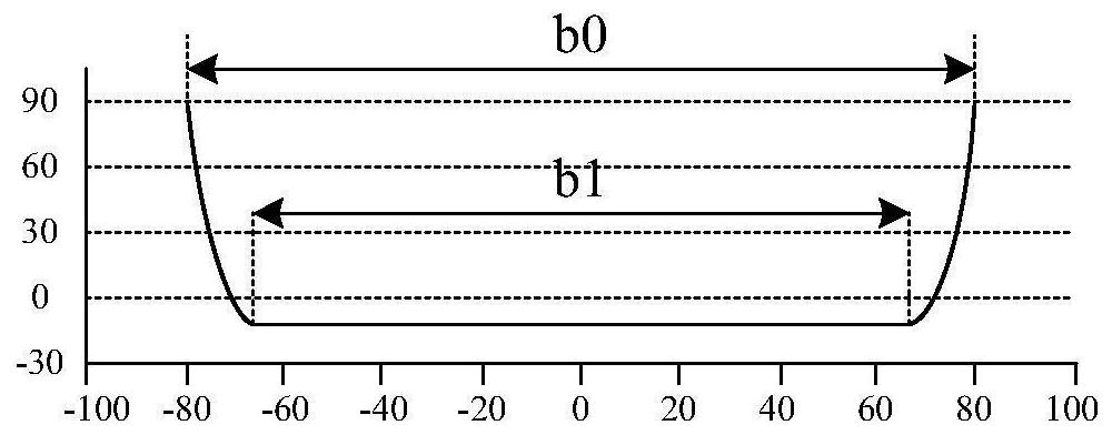
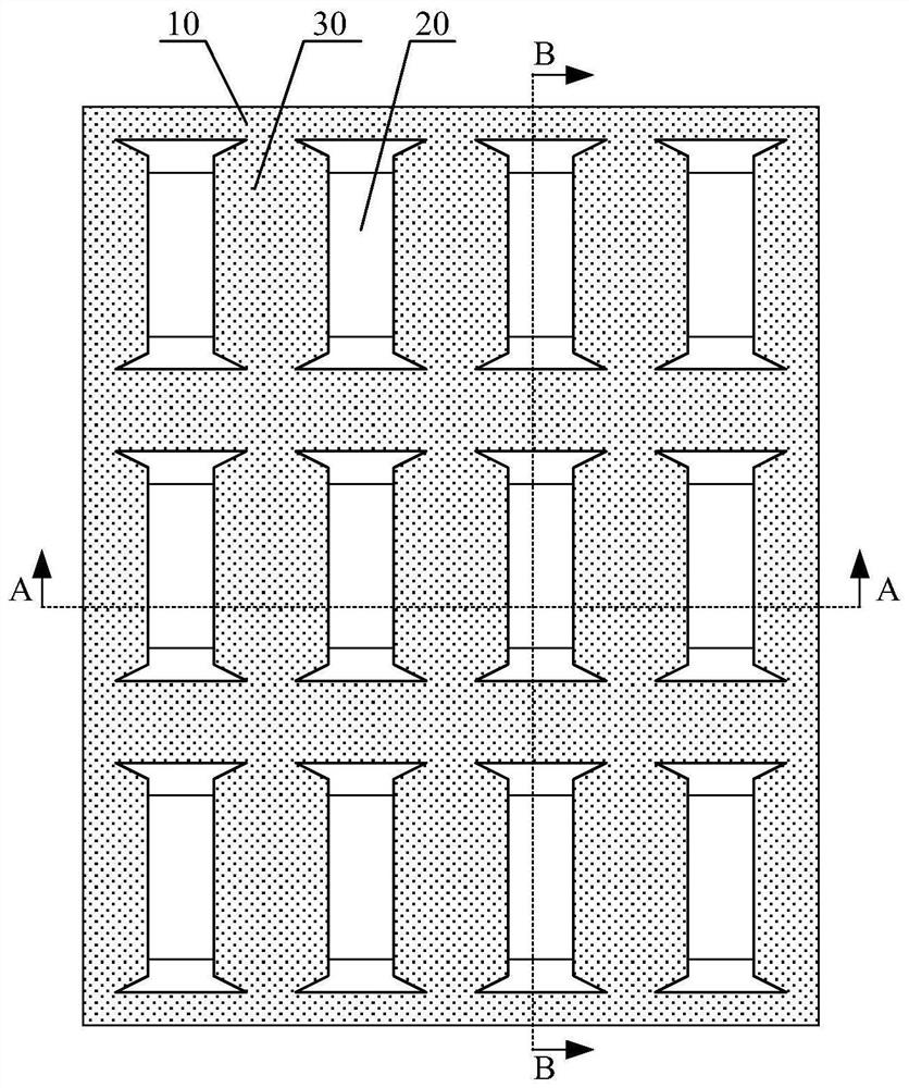
[0049] figure 2 It is a schematic structural view of the organic light emitting diode substrate according to the first embodiment of the present invention. image 3 for figure 2 Schematic diagram of the A-A cross-sectional structure. Figure 4 for figure 2 Schematic diagram of the B-B cross-sectional structure. The substrate includes a base 10 and a pixel defining layer 30 disposed on the base 10 to define a plurality of pixel regions 20 . from figure 2 It can be seen from the figure that the pixel area 20 is in the shape of a rectangle, A-A is along the short axis of the pixel area 20 ie the first direction, and B-B is along the long axis of the pixel area 20 ie the second direction. In the first direction, the width of the bottom of the cross section of the pixel defining layer 30 is smaller than the width of the top, such as image 3 shown. In the second direction, the width of the bottom of the cross section of the pixel defining layer 30 is greater than the wid...
no. 2 example
[0066] The main structure of the substrate of the second embodiment of the present invention is the same as that of the first embodiment. The difference is that, in the first direction, the two sides of the cross-section of the pixel defining layer protrude toward the pixel area. curve, such as Image 6 as shown, Image 6 It is a schematic diagram of the A-A cross-sectional structure of the substrate of the second embodiment of the present invention. from Image 6It can be seen from the figure that, in the first direction, the two sides of the cross-section of the pixel defining layer 30 are curves protruding toward the pixel area 20 , and it is easy to understand that the curve can be a parabola. Compared with a straight line, such a side shape is easier to cover the solution at the bottom of the pixel region 20, further slowing down the solvent evaporation, further reducing the airflow loss velocity in the first direction, and further improving the organic light-emitting l...
no. 3 example
[0083] Figure 9 It is a schematic diagram of the A-A cross-sectional structure of the substrate of the third embodiment of the present invention. The main structure of the substrate of the third embodiment of the present invention is the same as that of the first embodiment. The difference is that, in the first direction, one side of the cross-section of the pixel defining layer is a straight line, and is connected to the pixel defining layer. The angle formed by the bottom edge of the cross-section is 105°-135°, and the other side is a straight line, which is perpendicular to the bottom edge of the cross-section of the pixel defining layer. like Figure 9 As shown, in the first direction, the side 31 of the cross-section of the pixel defining layer 30 is a straight line, and the angle formed by the side 31 and the bottom is α, α is greater than 90°, preferably α is 105°˜135°. The other side 31' is also a straight line, and the angle between the side 31' and the bottom is α...
PUM
| Property | Measurement | Unit |
|---|---|---|
| height | aaaaa | aaaaa |
| thickness | aaaaa | aaaaa |
Abstract
Description
Claims
Application Information
 - R&D
- Intellectual Property
- Life Sciences
- Materials
- Tech Scout
- Unparalleled Data Quality
- Higher Quality Content
- 60% Fewer Hallucinations
Browse by: Latest US Patents, China's latest patents, Technical Efficacy Thesaurus, Application Domain, Technology Topic, Popular Technical Reports.
© 2025 PatSnap. All rights reserved.Legal|Privacy policy|Modern Slavery Act Transparency Statement|Sitemap|About US| Contact US: help@patsnap.com