OLED backplane structure and OLED backplane manufacturing method

A manufacturing method and backplane technology, applied in the field of OLED display, can solve the problems of limited effect, large conduction resistance of OLED display, high energy consumption of OLED display, etc., and achieve the effects of reducing energy consumption, eliminating metal annealing treatment, and simplifying the manufacturing process

Active Publication Date: 2020-06-26
WUHAN CHINA STAR OPTOELECTRONICS SEMICON DISPLAY TECH CO LTD
View PDF9 Cites 0 Cited by
  • Summary
  • Abstract
  • Description
  • Claims
  • Application Information

AI Technical Summary

Problems solved by technology

The superposition of these two types of contact resistance will lead to a larger on-resistance of the OLED display, so that the energy consumption of the OLED display is higher
[0010] Reducing the on-resistance is a key factor for reducing the energy consumption of OLED displays. One of the existing methods for reducing the on-resistance of OLED displays is to make a contact between the source 104 and the semiconductor layer 101 and between the drain 105 and the semiconductor layer 101. Add a certain thickness of insulating non-metal oxide dielectric layer, such as silicon oxide (SiOx), silicon nitride (SiNx), etc., to form a metal-interfacial layer-semiconductor structure (Metal-Interfacial layer-Semiconductor, MIS), to Reduce the Fermi level pinning effect, but the insulation of the dielectric layer will cause the dielectric layer itself to cause additional resistance in series; the second is to perform metal annealing after the anode 300 is fabricated to release the stress of the materials of each structural layer, so as to Reduce the contact resistance between the anode 300 and the drain 105 of the TFT 10, but the effect is limited

Method used


Image

  • OLED backplane structure and OLED backplane manufacturing method
  • OLED backplane structure and OLED backplane manufacturing method
  • OLED backplane structure and OLED backplane manufacturing method

Examples


Embodiment Construction

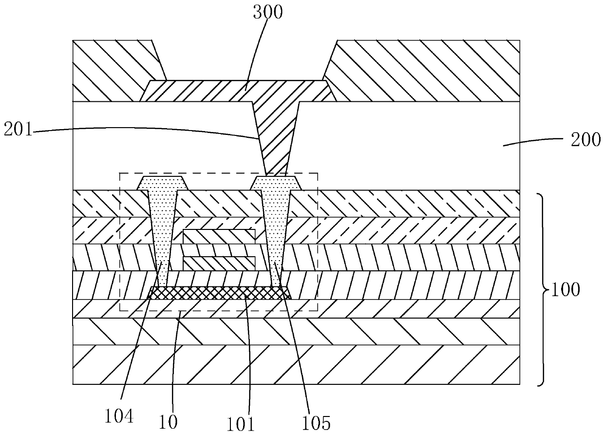
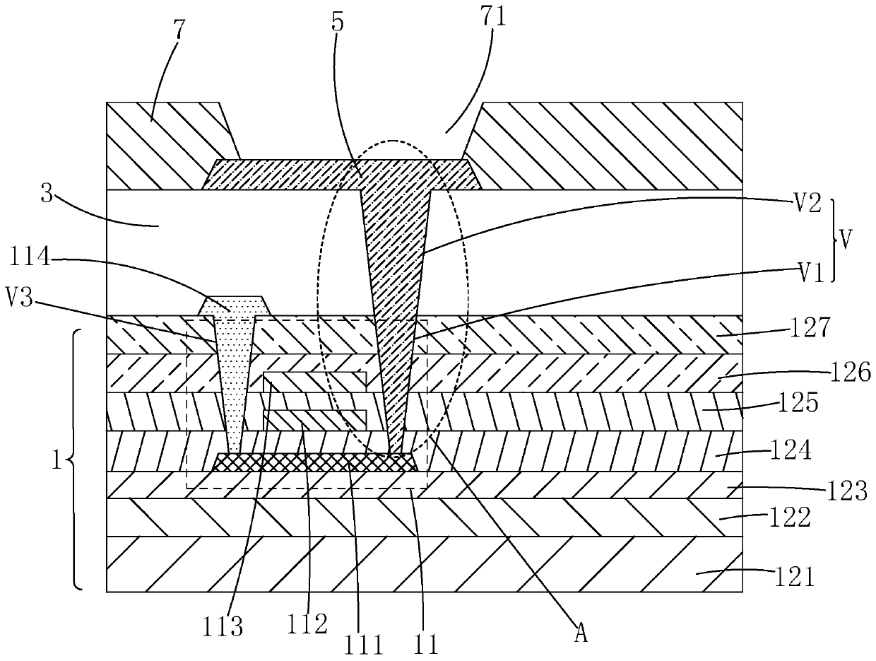
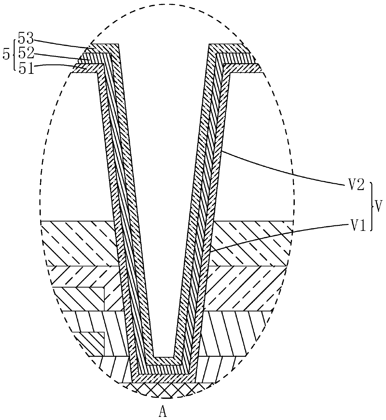
[0044] In order to further illustrate the technical means adopted by the present invention and its effects, a detailed description is given below in conjunction with the preferred embodiments of the present invention and the accompanying drawings. It should be noted that the accompanying drawings in this application are only schematic diagrams. Unless otherwise specified, they do not mean that the actual thickness ratio, flatness, and shape of each film layer are the same as those shown in the drawings. Restriction, the actual product may be different from the schematic diagram, for example, the shape of the hole and the shape of the combined part of each film layer will be different from the schematic diagram, which can be understood and known by those skilled in the art. The description of the sequence of process steps and the structure of the film layers in this application only represents the sequence and relative positions of the steps and the film layers directly related ...


PUM


Abstract

The invention provides an OLED backplane structure and an OLED backplane manufacturing method. The OLED backplane structure is provided with a composite electrode (5), on the one hand, the material of the part (51) of the composite electrode (5) in contact with the semiconductor layer (111) of the thin film transistor (11) is conductive metal oxide material, while reducing the Fermi level pinning effect between the metal and the semiconductor, it will not cause a large series resistance, and can greatly reduce the contact resistance of the metal-semiconductor. On the other hand, the anode and the thin film transistor ( The drain of 11) is integrated to eliminate the contact resistance between the anode and the drain of the thin film transistor (11), thereby greatly reducing the on-resistance of the OLED display and reducing energy consumption.

Description

technical field [0001] The present invention relates to the technical field of OLED display, in particular to an OLED backplane structure and a method for manufacturing the OLED backplane. Background technique [0002] In the field of display technology, flat panel display technologies such as Liquid Crystal Display (LCD) and Organic Light Emitting Diode (OLED) have gradually replaced CRT displays. Among them, OLED displays have many advantages such as self-luminescence, low driving voltage, high luminous efficiency, short response time, high definition and contrast, nearly 180° viewing angle, wide operating temperature range, flexible display and large-area full-color display, etc. It is recognized by the industry as the most promising display device. [0003] The OLED backplane is an important part of an OLED display. OLED backplanes typically include: [0004] An array substrate, wherein a plurality of thin film transistors (Thin Film Transistors, TFTs) arranged in an ...

Claims


Application Information

Patent Timeline
Patent Type & Authority Patents(China)
IPC IPC(8): H01L27/32H01L51/56
CPCH10K59/1315H10K71/00
Inventor 张伟彬
Owner WUHAN CHINA STAR OPTOELECTRONICS SEMICON DISPLAY TECH CO LTD
Why Eureka
Try Eureka