A method of manufacturing a semiconductor device

A manufacturing method and semiconductor technology, applied in semiconductor devices, semiconductor/solid-state device manufacturing, semiconductor/solid-state device components, etc., can solve problems such as increased difficulty in manufacturing process, easy generation of thermal stress, mismatch of thermal expansion coefficients, etc., and achieve reduction Effect of thermal stress, improvement of production efficiency, effect of guaranteed performance

Active Publication Date: 2020-03-10
SEMICON MFG INT (SHANGHAI) CORP +1
View PDF3 Cites 0 Cited by
  • Summary
  • Abstract
  • Description
  • Claims
  • Application Information

AI Technical Summary

Problems solved by technology

Due to the mismatch of the coefficient of thermal expansion (CTE) between the materials of the various components of the package, thermal stress is easily generated during the high temperature reflow process of the FCFBGA, resulting in warpage
Warping can easily cause poor contact between the chip and the package substrate, short circuit or open circuit, and further lead to failure of semiconductor devices
In addition, warpage will also make the subsequent process more difficult, leading to an increase in the process defect rate

Method used


Image

  • A method of manufacturing a semiconductor device
  • A method of manufacturing a semiconductor device
  • A method of manufacturing a semiconductor device

Examples


Embodiment 1

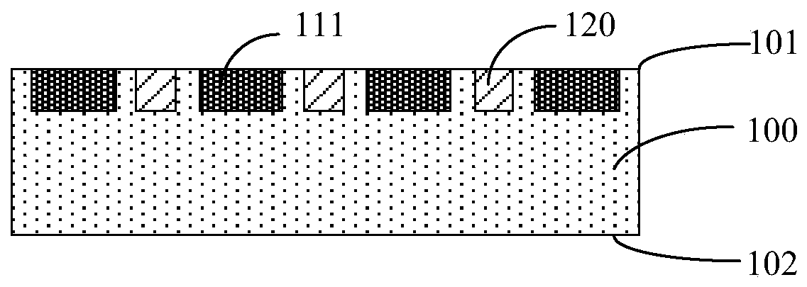
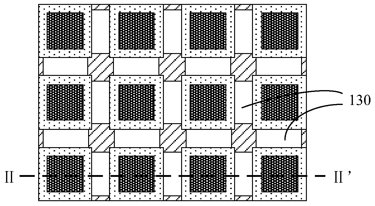
[0039] Refer below Figure 1A , 1B and Figure 2A , 2B , 2C, where Figure 1A is a schematic top view of a package substrate provided according to an exemplary embodiment of the present invention, Figure 1B is along Figure 1A The cross-sectional view taken along the line I-I', Figure 2A is a schematic top view of the package substrate obtained by the method according to the first exemplary embodiment of the present invention, Figure 2B is along Figure 2A The cross-sectional view taken along the line II-II'. Figure 2C yes Figure 2A A partial enlargement of the .

[0040] Next, specific implementations of the manufacturing method of the semiconductor device of the present invention will be described in detail.

[0041] First, a packaging substrate 100 is provided, the packaging substrate 100 has a first surface 101 and a second surface 102 opposite to each other, a plurality of chip prepackaging regions 110 are arranged on the first surface 101 and a plurality of c...

Embodiment 2

[0054] Refer below Figure 1A , 1B and Figure 3A , 3B ,in Figure 1A is a schematic top view of a package substrate provided according to an exemplary embodiment of the present invention, Figure 1B is along Figure 1A The cross-sectional view taken along the line I-I', Figure 3A is a schematic top view of the package substrate obtained by the method according to the second exemplary embodiment of the present invention, Figure 3B is along Figure 3A The cross-sectional view taken along the line III-III'.

[0055] Next, specific implementations of the manufacturing method of the semiconductor device of the present invention will be described in detail.

[0056] First, a packaging substrate 100 is provided, the packaging substrate 100 has a first surface 101 and a second surface 102 opposite to each other, a plurality of chip prepackaging regions 110 are arranged on the first surface 101 and a plurality of chips are located Strips 120 between the prepackaged areas.

[...


PUM


Abstract

The invention provides a fabrication method of a semiconductor device. The method comprises the steps of providing a package substrate, wherein the package substrate is provided with a first surface and a second surface which are opposite to each other, a plurality of chip pre-package regions and strip-shaped regions are arranged on the first surface, and the strip-shaped regions are arranged among the plurality of chip pre-package regions; and at least etching to remove a part of the strip-shaped regions. According to the fabrication method of the semiconductor device, provided by the invention, the thermal stress influence among the chip pre-package regions caused by thermal expansion coefficient mismatching of a package material is reduced by partially etching the package substrate, wraping is prevented, so that the performance stability of the semiconductor device is ensured, and the production efficiency is improved.

Description

technical field [0001] The invention relates to the technical field of semiconductors, in particular to a method for manufacturing a semiconductor device. Background technique [0002] Among semiconductor processes, a packaging process is used to electrically connect a semiconductor chip with a packaging substrate, and to package the semiconductor chip with a molding material to protect the semiconductor chip from an external environment. In recent years, due to the rapid development of digital network communication systems, the demand for high-performance and small-sized electronic systems has continued to increase, and integrated circuit packaging tends to be thinner and smaller. Ball Grid Array (BGA), as a widely used packaging technology, is characterized by the use of a package substrate with a semiconductor chip mounted on the chip side and a grid of solder balls mounted on the lower surface of the package substrate array. During the surface mount technology process,...

Claims


Application Information

Patent Timeline
Patent Type & Authority Patents(China)
IPC IPC(8): H01L21/56H01L23/12H01L23/13
CPCH01L21/561H01L23/12H01L23/13
Inventor 陆水华费春潮陆丽辉王亚平
Owner SEMICON MFG INT (SHANGHAI) CORP
Why Eureka
Try Eureka