
Electrostatic protection device based on SOI (Silicon-On-Insulator) technology and formed electrostatic protection circuit

An electrostatic protection and device technology, applied in the direction of electric solid devices, circuits, electrical components, etc., can solve the problems of small discharge capacity per unit size, insufficient ESD protection capacity, multi-layout area, etc., and achieve fast ESD response speed and reverse ESD The effect of enhanced protection

Inactive Publication Date: 2018-05-22
SHANGHAI INST OF MICROSYSTEM & INFORMATION TECH CHINESE ACAD OF SCI
View PDF3 Cites 5 Cited by
  • Summary
  • Abstract
  • Description
  • Claims
  • Application Information

AI Technical Summary

Problems solved by technology

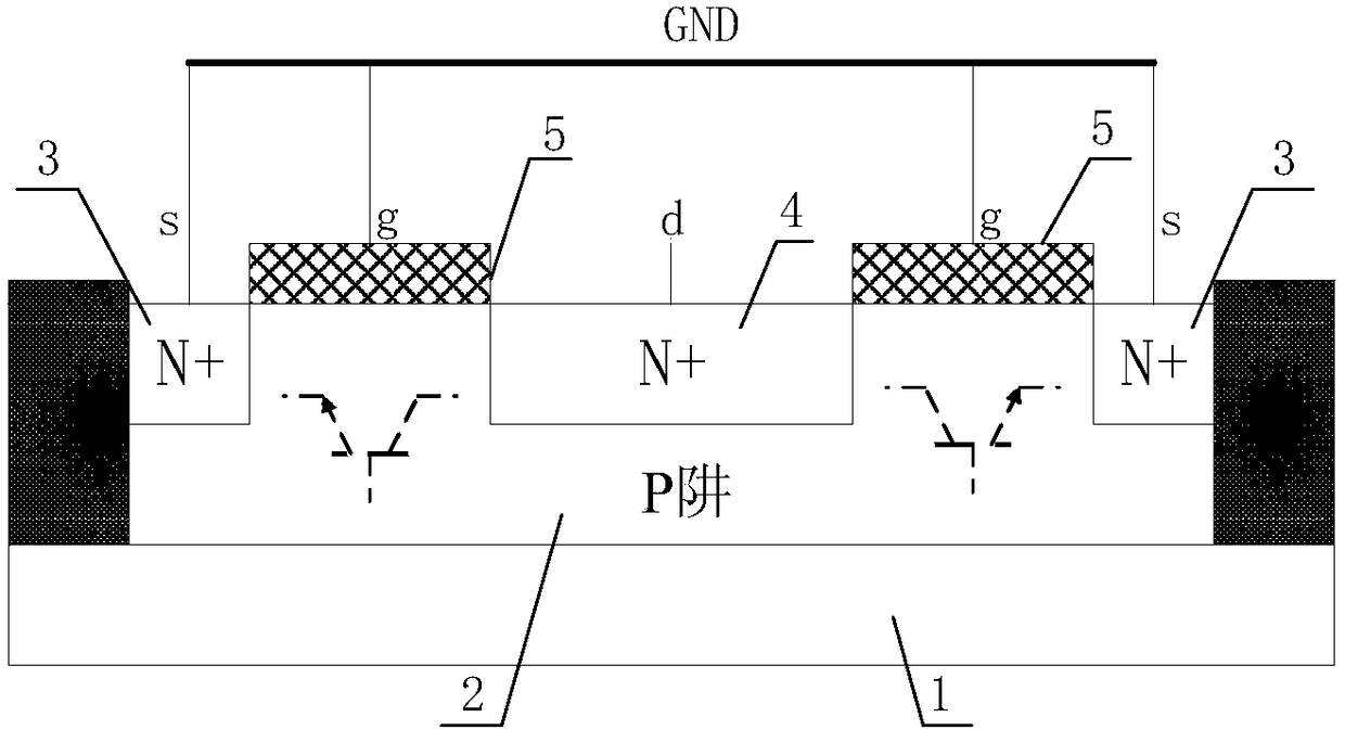
[0005] When a negative ESD pulse is applied to the drain 4 and the source is grounded, the source-P well forms a reverse-biased PN junction, and the P-well-drain forms a forward-biased PN junction. The conduction mechanism is the same as that described in the previous section. It means that the parallel structure is triggered as uniformly as possible, and the width of the source 3 also needs to be elongated, which requires more layout area
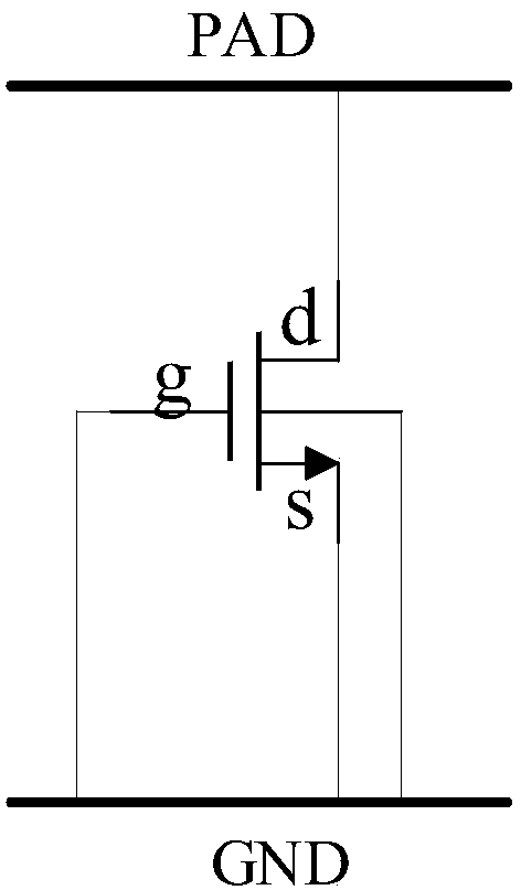
[0006] To sum up, the ESD protection of the traditional GGNMOS structure mainly relies on parasitic NPN, and the discharge capacity per unit size of the parasitic NPN is small, resulting in insufficient ESD protection capability.

Method used


Image

  • Electrostatic protection device based on SOI (Silicon-On-Insulator) technology and formed electrostatic protection circuit
  • Electrostatic protection device based on SOI (Silicon-On-Insulator) technology and formed electrostatic protection circuit
  • Electrostatic protection device based on SOI (Silicon-On-Insulator) technology and formed electrostatic protection circuit

Examples


Embodiment Construction

[0022] In order to make the present invention more comprehensible, preferred embodiments are described in detail below in conjunction with the accompanying drawings.

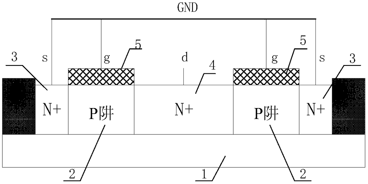
[0023] Figure 4 , Figure 5 Two embodiments of the improved electrostatic protection device of the present invention are given. and figure 2 , image 3 The structure comparison shows that the present invention adds a P+ contact region 6 and a dummy gate (dummy gate) 7 on the basis of the traditional multi-finger parallel GGNMOS. Wherein, the P+ contact region 6 is arranged on the side of the source 3 away from the drain 4, and the P+ contact region 6 and the source 3 are separated by the P well region 2; the dummy gate 7 covers the P+ contact region 6 and the source 3. on the P well region 2 between the source electrodes 3 . Since the P+ contact region 6 and the P well region 2 are connected, the P well region 2 can be electrically connected to the outside through the P+ contact region 6 (connected to GND...


PUM


Abstract

The invention provides an electrostatic protection device based on a SOI (Silicon-On-Insulator) technology and a formed electrostatic protection circuit. The device is a GGNMOS with a multiple parallel structure, and comprises a buried oxide layer, a P well area, a source, a drain, a gate, a P+ contact area and a pseudo gate, wherein the P+ contact area is arranged at one side, far away from the drain, of the source; the P+ contact area is separated from the source through the P well area; and the pseudo gate covers the P well area between the P+ contact area and the source. Thus, the reverseESD protection capability can be improved.

Description

technical field [0001] The invention relates to the field of integrated circuits, in particular to an SOI technology-based electrostatic protection device and an electrostatic protection circuit formed thereof. Background technique [0002] Electrostatic protection (ESD) is an important link in integrated circuit (IC) design. As the technology becomes more and more advanced, especially in the new SOI (Silicon-On-Insulator, silicon on insulator) process, due to the buried oxide BOX), the thickness of the top silicon (Si) is much thinner than that of traditional CMOS technology, and the ESD current is usually very large, which makes it more difficult to discharge the ESD current, and the current tends to concentrate to make the heat dissipation problem more serious. Therefore, the device is more likely to be burned, causing its ESD protection capability to become a major bottleneck. [0003] Such as figure 1 As shown, it is a commonly used Gate-Ground NMOS (GGNMOS for short)...

Claims


Application Information

Patent Timeline
IPC IPC(8): H01L27/02H01L29/423
CPCH01L27/0262H01L29/42316
Inventor 单毅董业民
Owner SHANGHAI INST OF MICROSYSTEM & INFORMATION TECH CHINESE ACAD OF SCI
Learn More