Green light organic electroluminescence device

A luminescent and electromechanical technology, applied in the field of organic electroluminescent devices, can solve the problems of high doping concentration, high cost, and low energy of the green OLED light-emitting layer, so as to improve device efficiency and life, improve efficiency, and improve excitation The effect of sub-utilization

Active Publication Date: 2018-05-08
KUNSHAN NEW FLAT PANEL DISPLAY TECH CENT
View PDF3 Cites 10 Cited by
  • Summary
  • Abstract
  • Description
  • Claims
  • Application Information

AI Technical Summary

Problems solved by technology

[0007] Therefore, the technical problem to be solved by the present invention lies in the problems of low energy, high doping concentration, and high cost of the green OLED light-emitting layer in the prior art, and further provides a green organic electroluminescent device, which uses thermally activated delayed fluorescence material as the main material, using The energy transfer method reduces the doping concentration of the dye, thereby improving the life and efficiency of the device

Method used


Image

  • Green light organic electroluminescence device
  • Green light organic electroluminescence device
  • Green light organic electroluminescence device

Examples


Embodiment 1

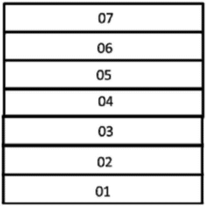
[0070] like image 3 As shown, a green organic electroluminescent device provided by the present invention includes a substrate, and a first electrode layer 01, a light emitting layer 04, and a second electrode layer 07 sequentially formed on the substrate, the first electrode A first organic functional layer is arranged between the layer 01 and the light-emitting layer 04 , and a second organic functional layer is arranged between the light-emitting layer 04 and the second electrode layer 07 . The first organic functional layer is the hole injection layer 02 and / or the hole transport layer 03 , and the second organic functional layer is the electron transport layer 05 and / or the electron injection layer 06 .

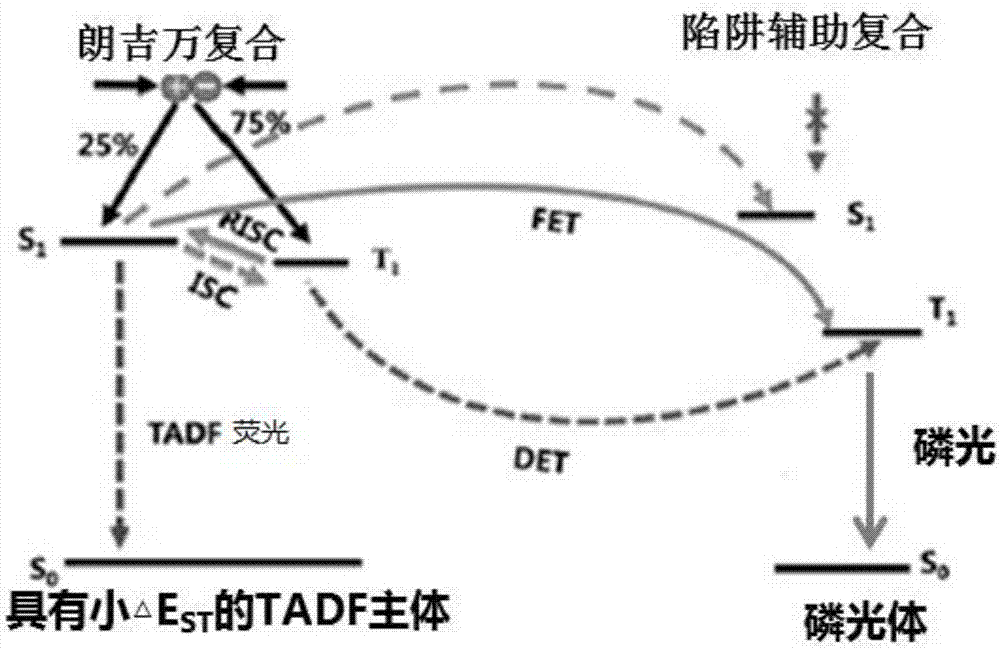
[0071] The light-emitting host material of the device in this embodiment is a thermally activated delayed fluorescent material and a hole-type transport material doped or not doped with a hole-type transport material, and the mass ratio of the thermally activated delaye...

Embodiment 2

[0081] The structures of the light-emitting devices from device 2 to device 5 are the same as those of device 1, except that the doping concentration of the green phosphorescent dye is different. Its structure is as follows:

[0082] ITO / NPB(40nm) / TCTA(10nm) / Formula 2-1: 0.5~5wt%Ir(ppy) 2 (acac)(20nm) / Bphen(40nm) / LiF(5nm) / Al

[0083] Table 3 Performance test results of device 2 to device 5

[0084]

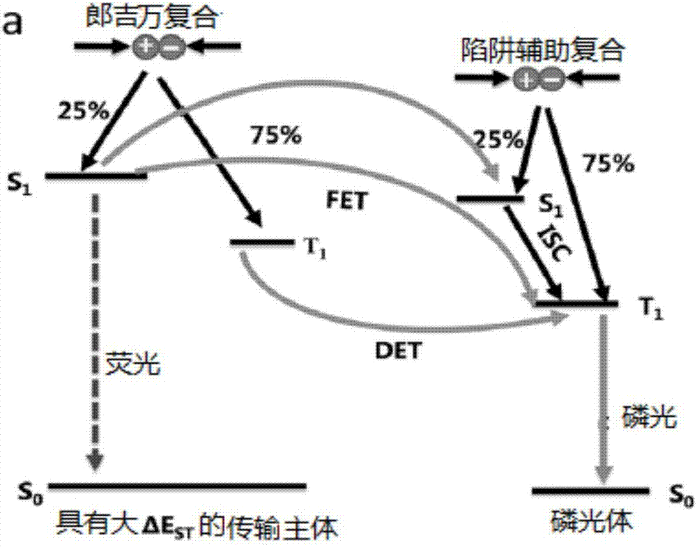
[0085] The performance of light-emitting devices from device 2 to device 5 was tested, as shown in Table 3, at 5000cd / m 2 Under brightness, as the doping concentration of the dye increases, the current efficiency of the device also increases, because the long-range The energy transfer improves the exciton utilization, which in turn increases the device efficiency.

Embodiment 3

[0087] The structures of the light-emitting devices from device 6 to device 10 are the same as those of the light-emitting device in Embodiment 1, except that the host material of the light-emitting layer 06 is different. Its structure is as follows:

[0088] ITO / NPB(40nm) / TCTA(10nm) / host material: 3wt%Ir(ppy) 2 (acac)(20nm) / Bphen(40nm) / LiF(5nm) / Al

[0089] Table 4 Performance test results of device 6 to device 10

[0090]

[0091]The performance of light-emitting devices from device 6 to device 10 was tested, as shown in Table 4, at 5000cd / m 2 Under the brightness, different thermally activated delayed fluorescent materials and different hole-type transport materials were co-evaporated. Although the doping ratios were different, the device performance showed low driving voltage and high efficiency, indicating that the thermally activated delayed Fluorescence: The host material composed of hole-transport materials is universal, and its devices have high-efficiency perfor...


PUM

PropertyMeasurementUnit
Thicknessaaaaaaaaaa

Abstract

The invention discloses a green light organic electroluminescence device. The device includes a substrate, and a first electrode layer, a light emitting layer and a second electrode layer formed on the substrate in sequence. The light emitting layer includes body material and a green phosphorescence dye. The body material is thermal activation delayed fluorescence material (TADF) doped or not doped with cavity-type transmission material and the cavity-type transmission material. The mass ratio between the thermal activation delayed fluorescence material and the cavity-type transmission material is (0.1-100%):(99.9%-0%). The doping proportion of the green phosphorescence dye in the green phosphorescence dye is 0.5-10 wt%. According to the invention, Forster energy transfer is adopted for reducing TTA (Triplet State-Triplet State Annihilation), improving exciton utilization rate and further improving device efficiency and service life. The Delta E<ST> of the device provided by the invention is low (<0.3eV). The electron accepter stability is good and the torsion angle between accepters and donors is smaller and the radiative transmission rate is high. The single state S1 of the thermal activation delayed fluorescence material is lower than the single state S1 of a common subject and device drive voltage can be reduced effectively.

Description

technical field [0001] The invention relates to the technical field of organic electroluminescent devices, in particular to a green organic electroluminescent device using heat-activated delayed fluorescent materials and hole-type transport materials as light-emitting host materials. Background technique [0002] After nearly 30 years of development, organic electroluminescent devices (English full name Organic Light Emitting Device, referred to as OLED) as the next generation of lighting and display technology, has a wide color gamut, fast response, wide viewing angle, no pollution, high contrast, Advantages such as planarization have been applied to a certain extent in lighting and display. [0003] Organic electroluminescent devices usually include a cathode, a light-emitting layer and an anode, and the light-emitting layer includes a light-emitting host material and a light-emitting dye, such as figure 1 As shown, under the condition of electro-excitation, the organic e...

Claims


Application Information

Patent Timeline
IPC IPC(8): H01L51/00H01L51/50
CPCH10K85/60H10K50/12
Inventor 赵菲段炼张东东刘嵩
Owner KUNSHAN NEW FLAT PANEL DISPLAY TECH CENT
Why Eureka
Try Eureka