A kind of white light led packaging method

A technology of LED packaging and LED wicks, applied in semiconductor devices, electrical components, circuits, etc., can solve the problems of decreasing quantum efficiency, decreasing light intensity, affecting heat dissipation, etc., to increase heat dissipation effect, improve light transmittance, and increase channels. Effect

Active Publication Date: 2020-06-30
广州市安亿仕电子科技有限公司
View PDF6 Cites 0 Cited by
  • Summary
  • Abstract
  • Description
  • Claims
  • Application Information

AI Technical Summary

Problems solved by technology

First of all, the light emitted by the LED light source is generally distributed in a divergent manner, that is, the Lambertian distribution, which leads to insufficient illumination brightness of the light source, and generally requires secondary shaping through an external lens to meet the lighting needs of specific occasions, thus increasing production costs; secondly , in the current high-power LED packaging structure, the phosphor is generally directly coated on the surface of the chip. Since the chip has an absorption effect on the backscattered light, this direct coating method will reduce the light extraction efficiency of the package. , In addition, the high temperature generated by the chip will significantly reduce the quantum efficiency of the phosphor, which seriously affects the lumen efficiency of the package; again, only a part of the energy in the LED input power is converted into light energy, and the rest of the energy is converted into heat energy, so For LED chips, especially LED chips with high power density, how to control their energy is an important issue that LED manufacturers and lamps should focus on solving; then, because high-power LEDs are used in lighting and other occasions, cost control is very important, and large The structural size of the external heat sink of the power LED lamp is not allowed to be too large, and it is impossible to allow active cooling by adding an electric fan. The safe junction temperature of the LED chip should be within 110°C. If the junction temperature is too high, it will cause light intensity. A series of problems, such as lowering, spectral shift, rising color temperature, increasing thermal stress, and accelerated aging of the chip, greatly reduce the service life of the LED. Light efficiency; finally, most of the chips are packaged on thin metal substrates. Since the metal substrate is thin, the heat capacity is small, and it is easy to deform, the contact between it and the bottom surface of the heat sink is not close enough to affect the heat dissipation effect.

Method used


Image

  • A kind of white light led packaging method
  • A kind of white light led packaging method
  • A kind of white light led packaging method

Examples


Embodiment 1

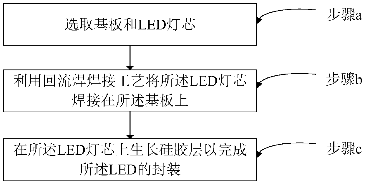
[0056] See figure 1 , figure 1It is a flow chart of a white LED packaging method provided by an embodiment of the present invention. The method comprises the steps of:

[0057] Step a, select substrate and LED wick;

[0058] Step b, using a reflow soldering process to weld the LED wick on the substrate;

[0059] Step c, growing a silica gel layer on the LED wick to complete the packaging of the LED.

[0060] Wherein, for selecting the substrate in step a, including:

[0061] Step a1, selecting a plate with a thickness of 0.5-10mm and made of copper;

[0062] Step a2, making a plurality of circular through holes along the width direction and parallel to the plane of the board in the board to form the substrate.

[0063] Further, making a plurality of circular through holes along the width direction and parallel to the plane of the sheet in the sheet in step a2 includes:

[0064] direct casting in the plate or directly drilling on the plate to make a plurality of circular...

Embodiment 2

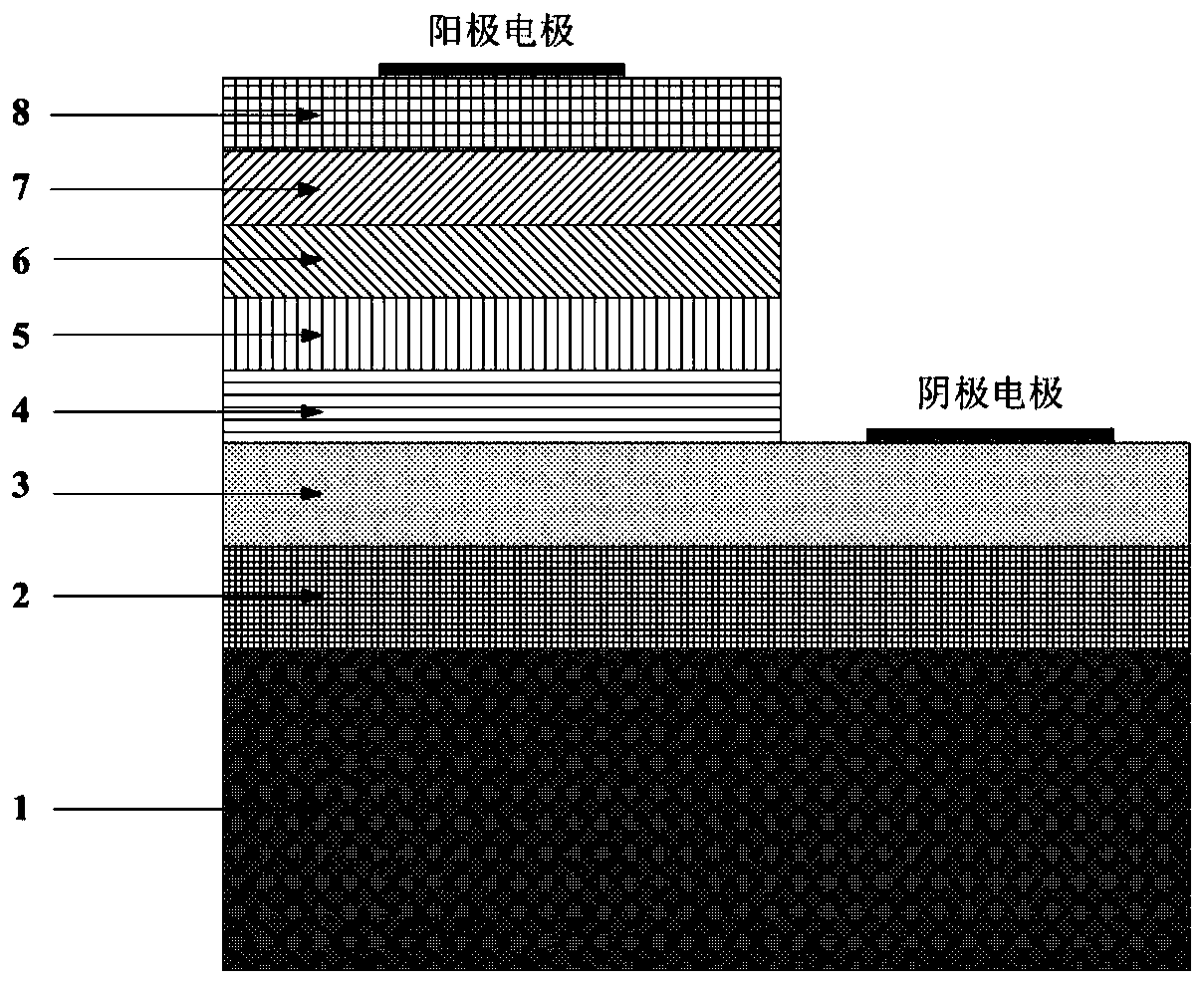
[0098] See figure 2 and image 3 , figure 2 A flow chart of another white LED packaging method provided by an embodiment of the present invention, image 3 It is a schematic structural diagram of a GaN-based blue light chip provided by an embodiment of the present invention. On the basis of the above embodiments, this embodiment will introduce the process flow of the present invention in more detail. The method includes:

[0099] S1, LED wick selection

[0100] The GaN-based blue light chip is selected as the LED wick, and the structure of the GaN-based blue light chip is as follows: image 3 As shown, the chip includes: substrate material 1, GaN buffer layer 2, N-type GaN layer 3, P-type GaN quantum well wide bandgap material 4, InGaN layer 5, P-type GaN quantum well wide bandgap material 6, AlGaN barrier layer Material 7, P-type GaN layer 8.

[0101] S2. Substrate selection

[0102] S21, support / substrate preparation

[0103] Metal copper is selected as the materi...

Embodiment 3

[0148] Please continue to see image 3 and also see Figure 4 , Figure 5 and Figure 6 , Figure 4 A schematic diagram of an LED package structure provided by an embodiment of the present invention; Figure 5 A schematic diagram of a substrate structure provided by an embodiment of the present invention; Figure 6 It is a schematic diagram of another LED package structure provided by the embodiment of the present invention. This embodiment introduces the LED packaging structure in detail on the basis of the above-mentioned embodiments. The LED packaging structure is as follows: Figure 4 As shown, it includes: a packaging substrate 21 with LED wicks, a lower layer of silica gel 22 , a hemispherical silica gel ball 23 , and an upper layer of silica gel 24 . Among them, the radius R of the hemispherical silica gel ball 23 is greater than 10 microns; the distance L between the hemispherical silica gel ball 23 and the LED wick is greater than 10 microns; the distance betwee...


PUM

PropertyMeasurementUnit
wavelengthaaaaaaaaaa
diameteraaaaaaaaaa
thicknessaaaaaaaaaa

Abstract

The invention relates to a white LED packaging method, which comprises the steps of selecting a substrate and an LED lamp core; welding the LED lamp core on the substrate by using a reflow soldering process; and growing silica gel layers on the LED lamp core to complete packaging of an LED. According to the white LED packaging method, the problem that the quantum efficiency of fluorescent powder is reduced due to high temperature is solved through separation of the fluorescent powder from the LED lamp core.

Description

technical field [0001] The invention relates to the technical field of packaging, in particular to a white LED packaging method. Background technique [0002] LED has the characteristics of long life, high luminous efficiency, good color rendering, safety and reliability, rich colors and easy maintenance. Under the background of increasingly serious environmental pollution, climate warming and increasingly tense energy sources, semiconductor lighting technology developed based on high-power LEDs has been recognized as one of the most promising high-tech fields in the 21st century. This is a great leap in the history of human lighting since gas lighting, incandescent lamps and fluorescent lamps, and has rapidly improved the lighting quality of human life. [0003] In recent years, LEDs mostly use a GaN-based blue wick plus yellow fluorescent light to generate white light to achieve lighting. This method has the following problems. First of all, the light emitted by the LED ...

Claims


Application Information

Patent Timeline
Patent Type & Authority Patents(China)
IPC IPC(8): H01L33/48H01L33/50H01L33/56H01L33/58H01L33/62H01L33/64
CPCH01L33/48H01L33/507H01L33/56H01L33/58H01L33/62H01L33/647H01L2933/0033H01L2933/0041H01L2933/005H01L2933/0058H01L2933/0066H01L2933/0075
Inventor 张亮
Owner 广州市安亿仕电子科技有限公司
Why Eureka
Try Eureka