A high-power blue LED multi-layer packaging structure

A packaging structure, high-power technology, applied in the direction of semiconductor devices, electrical components, circuits, etc., can solve the problems of decreased quantum efficiency of phosphor powder, affecting packaging lumen efficiency, reducing packaging light extraction efficiency, etc., to solve the problem of quantum efficiency decline, improve The effect of light source utilization and low cost

Active Publication Date: 2020-05-15
深圳市天瀛深源科技有限公司
View PDF3 Cites 0 Cited by
  • Summary
  • Abstract
  • Description
  • Claims
  • Application Information

AI Technical Summary

Problems solved by technology

Since the chip absorbs the backscattered light, this direct coating method will reduce the light extraction efficiency of the package
In addition, if the phosphor is directly coated on the chip, the high temperature generated by the chip will significantly reduce the quantum efficiency of the phosphor, which will seriously affect the lumen efficiency of the package.

Method used


Image

  • A high-power blue LED multi-layer packaging structure
  • A high-power blue LED multi-layer packaging structure
  • A high-power blue LED multi-layer packaging structure

Examples


Embodiment 1

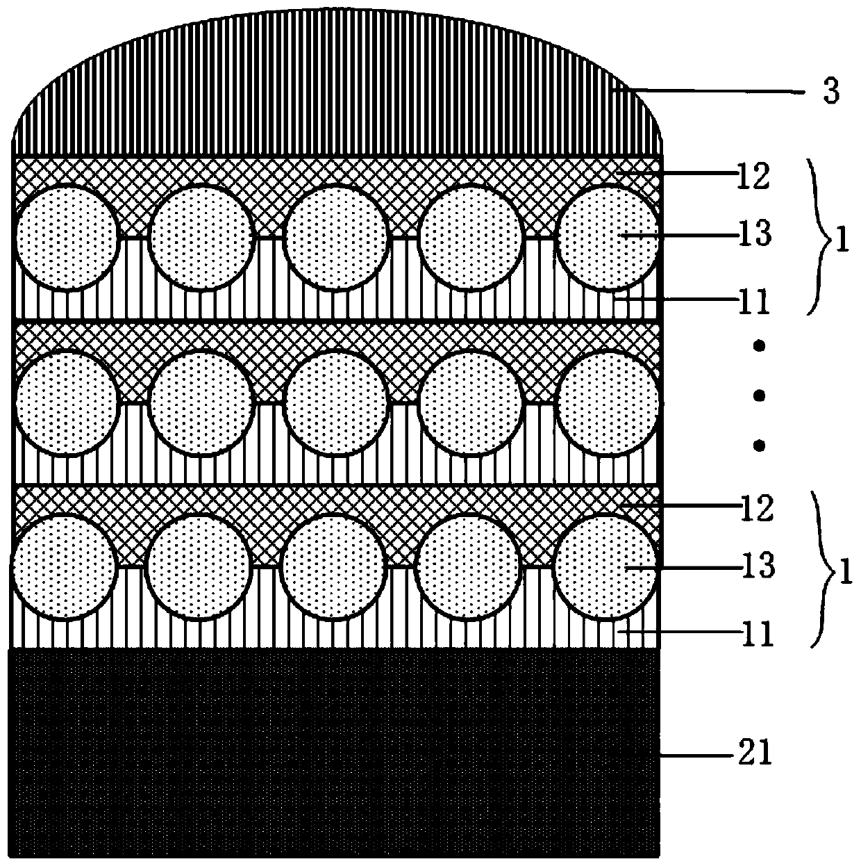
[0031] figure 1 A schematic diagram of a high-power blue LED multi-layer packaging structure provided by an embodiment of the present invention, including: multiple sets of lens layers 1, a heat dissipation substrate 21, and an outer packaging layer 3;

[0032] The lens layer 1 is arranged on the heat dissipation substrate 21, and an outer encapsulation layer 3 is arranged on the top of the multiple sets of lens layers 1; wherein, each set of lens layers includes a lower encapsulation layer 11, an upper encapsulation layer 12, a spherical lens 13;

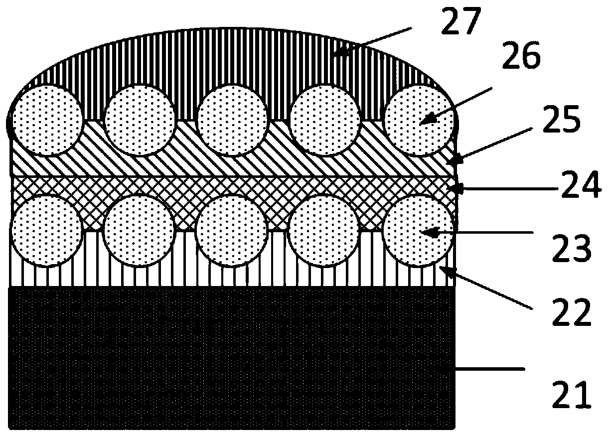
[0033] At least a part of the spherical lens 23 is embedded in the lower encapsulation layer 22 , and the upper encapsulation layer 24 is located on the non-embedded portion of the spherical lens 23 and the lower encapsulation layer 22 .

[0034] The lower encapsulation layer 11, the upper encapsulation layer 12, and the spherical lens 13 are all made of silica gel. The outer packaging layer 3 is a convex structure. Specifically...


PUM

PropertyMeasurementUnit
diameteraaaaaaaaaa
diameteraaaaaaaaaa
thicknessaaaaaaaaaa

Abstract

The invention discloses a multilayer packaging structure of a high-power blue-light LED. The structure comprises a plurality of groups of lens layers (1), a heat dissipation substrate (21) and an outer packaging layer (3). The lens layers (1) are arranged on the heat dissipation substrate (21). The outer packaging layer (3) is further arranged on the topmost part of the plurality of groups of lenslayers (1). Each group of the lens layers comprises a lower packaging layer (11), an upper packaging layer (12) and a spherical lens (13). At least a part of a spherical lens (23) is embedded into the lower packaging layer (22). The upper packaging layer (24) is located in the non-embedded part of the spherical lens (23) and is above the lower packaging layer (22). According to the multilayer packaging structure of the high-power blue-light LED provided in the invention, the spherical lens is adopted. Therefore, the technical problem that the illumination brightness of a light source is not centralized enough is solved. Meanwhile, the secondary shaping is not needed, so that the structure is simple. The production cost is reduced. In addition, compared with the prior art, fluorescent powders do not need to be coated on a chip. The problem that the brightness is reduced due to the fact that the quantum efficiency of fluorescent powders caused by high temperature is reduced is solved.

Description

technical field [0001] The invention belongs to the field of semiconductor packaging, and in particular relates to a high-power blue LED multilayer packaging structure. Background technique [0002] LED has the characteristics of long life, high luminous efficiency, good color rendering, safety and reliability, rich colors and easy maintenance. At present, LEDs mostly use GaN-based blue light wicks plus yellow fluorescent light to generate white light to achieve lighting. [0003] However, the prior art has the following drawbacks. [0004] 1. Since the light emitted by the LED light source is generally distributed in a divergent manner, that is, the Lambertian distribution, this causes the illumination brightness of the light source to be insufficiently concentrated. The existing silicone lens generally needs to be reshaped by an external lens to meet the lighting requirements of specific occasions. The structure is complicated and the production cost is higher. [0005]...

Claims


Application Information

Patent Timeline
Patent Type & Authority Patents(China)
IPC IPC(8): H01L33/58H01L33/54H01L33/64H01L33/50H01L33/56
CPCH01L33/507H01L33/54H01L33/56H01L33/58H01L33/641
Inventor 尹晓雪
Owner 深圳市天瀛深源科技有限公司
Why Eureka
Try Eureka