Eureka AIR delivers breakthrough ideas for toughest innovation challenges, trusted by R&D personnel around the world.

Flexible display panel and manufacturing method thereof

A flexible display and flexible substrate technology, applied in semiconductor/solid-state device manufacturing, electrical components, electric solid-state devices, etc., can solve problems such as cracks, edge substrate flatness wrinkles, and easy cracks, etc. Yield rate, anti-display effect and structural strength effect

Active Publication Date: 2018-04-13
BOE TECH GRP CO LTD
View PDF3 Cites 10 Cited by
  • Summary
  • Abstract
  • Description
  • Claims
  • Application Information

AI Technical Summary

Problems solved by technology

However, in this process, if the depth of the groove is too large, a part of the flexible substrate (such as PI substrate) will be etched away, resulting in wrinkles that affect the flatness of the edge substrate, and then cracks appear again.
[0004] In the prior art, multiple groove areas are designed at the edge of the non-display area, and the buffer layer, gate insulating layer, and interlayer dielectric layer in the flexible display panel are etched. However, if the etching conditions are not appropriate, etching will occur Excessive phenomenon, the flexible substrate will be etched, which will affect the flatness and local stress of the substrate in the edge area, which will lead to cracks easily

Method used

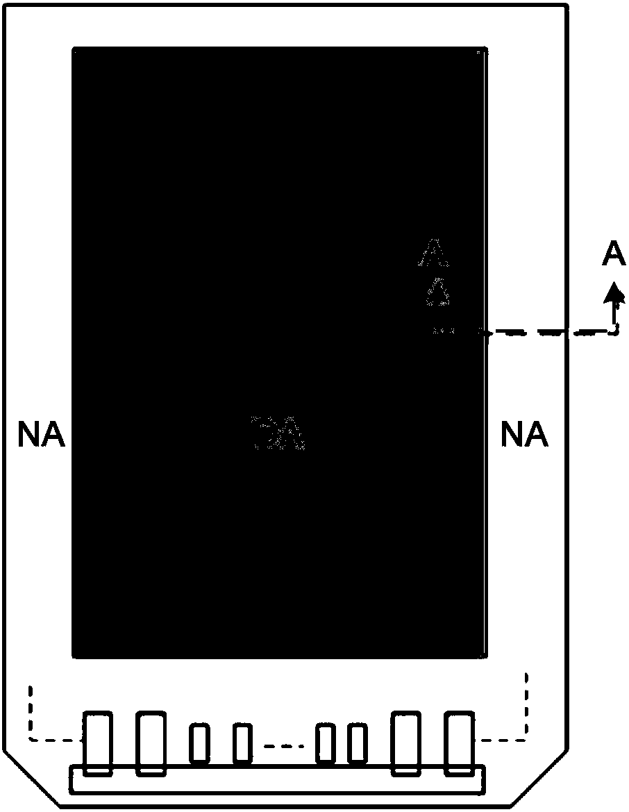
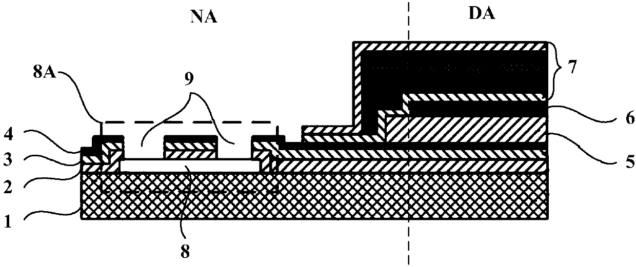
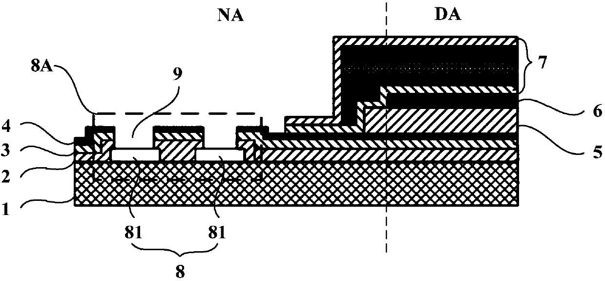

Image

  • Flexible display panel and manufacturing method thereof
  • Flexible display panel and manufacturing method thereof
  • Flexible display panel and manufacturing method thereof

Examples


Embodiment Construction

[0050] The following will clearly and completely describe the technical solutions in the embodiments of the present invention with reference to the accompanying drawings in the embodiments of the present invention. Obviously, the described embodiments are only some, not all, embodiments of the present invention. Based on the embodiments of the present invention, all other embodiments obtained by persons of ordinary skill in the art without making creative efforts belong to the protection scope of the present invention.

[0051] Please refer to figure 1 , figure 2 with image 3 , The flexible display panel provided by an embodiment of the present invention includes a flexible substrate 1, a buffer layer 2, a gate insulating layer 3, an interlayer dielectric layer 4, a thin film transistor 5, an organic electroluminescent element 6, and an encapsulation layer 7, wherein, The flexible substrate 1 includes a display area DA and a non-display area NA. The display area DA of the ...


PUM


Abstract

The invention discloses a flexible display panel and a manufacturing method thereof so that the possibility of excessive etching in groove hole etching in a non-display area of a flexible display panel can be reduced and thus the etching precision is improved and the yield of the flexible display panel is enhanced. The flexible display panel is composed of a flexible substrate, a buffer layer, a gate insulating layer, an interlayer dielectric layer, a thin-film transistor, an organic electroluminescence element, and an encapsulation layer. The flexible substrate consists of a display area anda non-display area. An etching stop layer is arranged at the display area of the flexible substrate; and the buffer layer, the gate insulating layer, and the interlayer dielectric layer are arranged on the flexible substrate and the etching stop layer successively. At least one etched groove hole is formed in a region, corresponding to the etching stop layer, of each of the buffer layer, the gateinsulating layer, and the interlayer dielectric layer in the non-display area respectively. And the thin-film transistor, the organic electroluminescence element, and the encapsulation layer are arranged on the interlayer dielectric layer in the display area successively.

Description

technical field [0001] The invention relates to the field of display technology, in particular to a flexible display panel and a manufacturing method. Background technique [0002] Compared with LCD devices, OLED (Organic Light Emission Display, organic electroluminescent diode) display devices have the characteristics of self-illumination, no need for backlight, and have the characteristics of good color and wide viewing angle, showing wider applications than LCD devices scope. Solid-state materials emit light to make the device design thinner and bendable, and it is the most potential technology for the development of flexible display devices. [0003] Compared with the preparation process of traditional OLED devices, the preparation process of flexible OLED devices is very compatible. The difference is that the flexible substrate process is added, and the packaging process and the module process of the packaging back end are changed at the same time. The substrate array...

Claims


Application Information

Patent Timeline
Patent Type & Authority Applications(China)
IPC IPC(8): H01L27/32H01L27/12H01L21/77
CPCH01L27/1218H01L27/1262H10K59/12H10K59/1201
Inventor 孙韬张嵩
Owner BOE TECH GRP CO LTD
Why Eureka
Eureka Blog
Learn More