Method for dry-etching silicon groove

A dry etching, silicon groove technology, applied in electrical components, semiconductor/solid-state device manufacturing, circuits, etc., can solve problems such as increased scrap rate, processing cost impact of processing cycle, device failure, etc., to reduce processing costs and reduce processing costs. The steps are clear and orderly, and the product quality is good

Inactive Publication Date: 2018-04-10
YANGZHOU YANGJIE ELECTRONIC TECH CO LTD
View PDF4 Cites 0 Cited by
  • Summary
  • Abstract
  • Description
  • Claims
  • Application Information

AI Technical Summary

Problems solved by technology

However, because the brominated polymer will continue to accumulate on the sidewalls of the silicon trench during production, excessive accumulation will cause the ions to re-sputter a large amount of the polymer onto the surface of the silicon, forming a large number of " "Silicon Grass", which causes device failure and brings a huge additional increase to the scrap rate
[0003] In addition, during the etching process of the silicon groove, a large amount of silicon-containing brominated polymers will adhere to the inner wall of the processing equipment, so that the operator needs to clean the processing equipment for the second time after processing, which will shorten the processing cycle and processing time. cost has a huge impact on

Method used


Image

  • Method for dry-etching silicon groove
  • Method for dry-etching silicon groove
  • Method for dry-etching silicon groove

Examples


Embodiment Construction

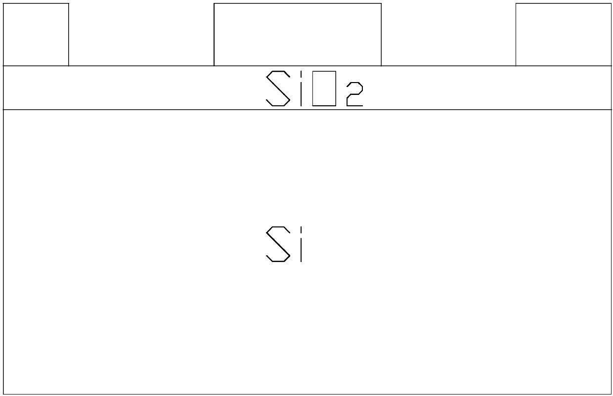
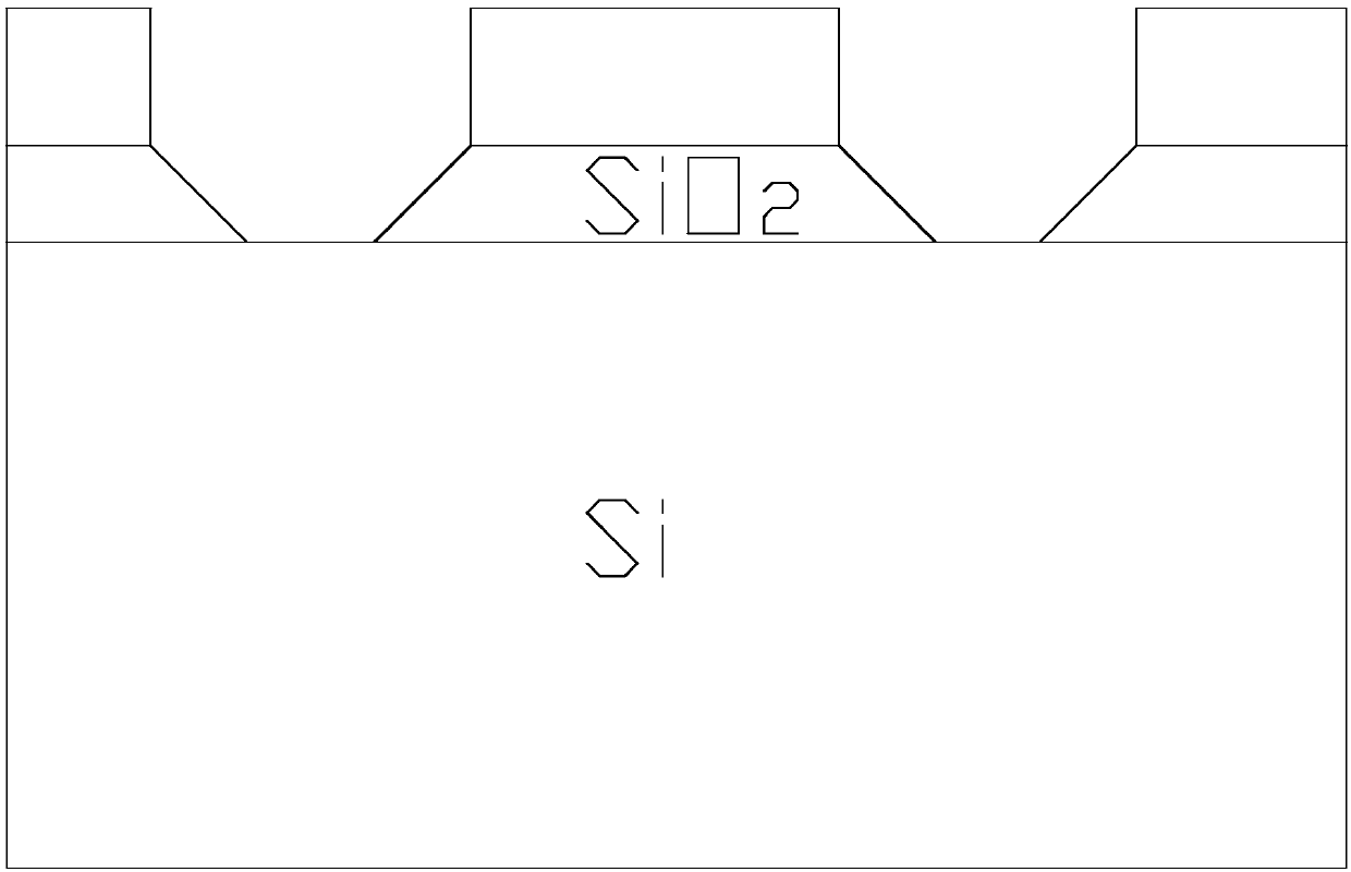
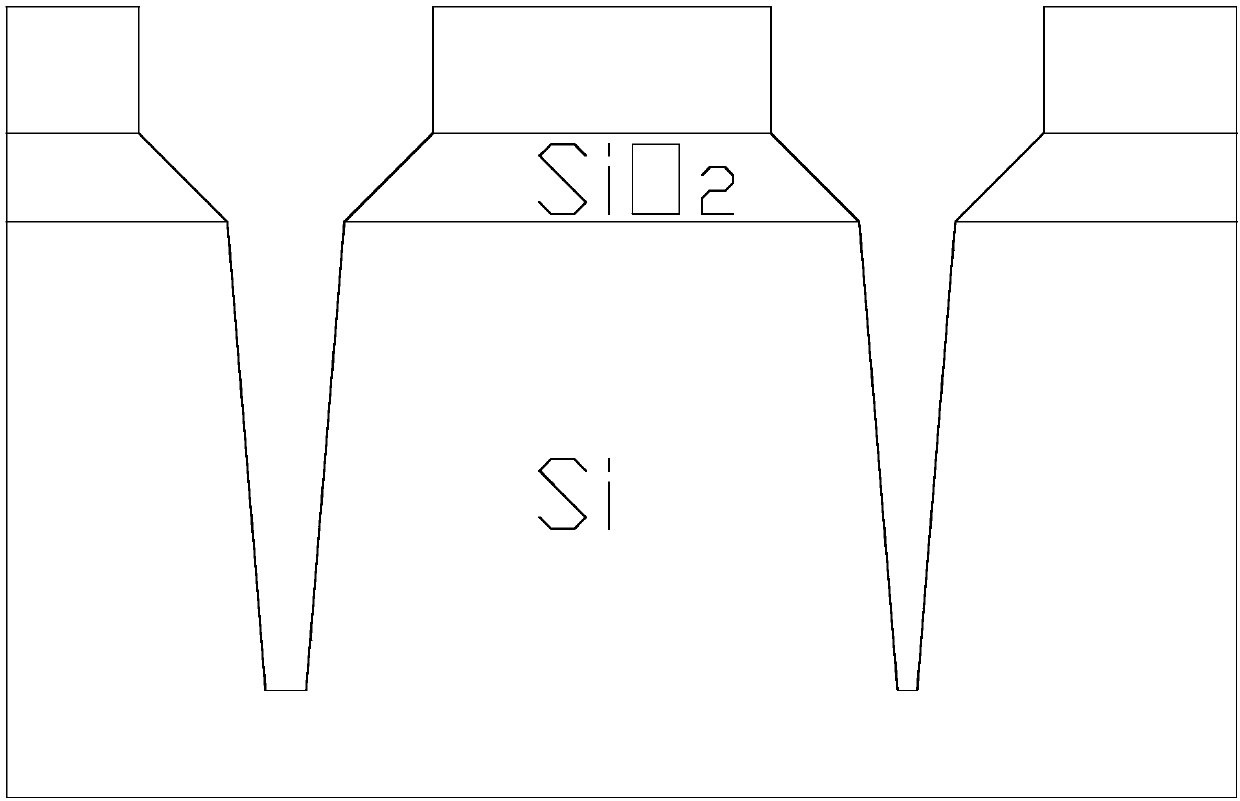
[0016] The invention as Figure 1-3 shown, follow the steps below:

[0017] 1) Place photoresist: place photoresist according to the position of the preset pattern;

[0018] 2) Preparation of mask layer: through Ar, CHF 3 、CF 4 Etching several trenches on the silicon oxide to form a mask layer;

[0019] 3), etching silicon groove: through Cl 2 , SF 6 , Ar physically etch silicon under the action of a high-frequency electric field; complete. Even with Cl 2 Add to SF 6 With the formulation of Ar, adjust the bombardment voltage (bias electric field) of the chassis to physically etch silicon. The formulation starts with Cl 2 , AR as the main body, SF 6 is fine-tuning, where SF 6 It is isotropic etching, but it can be used to fine-tune the rate of etching Si to meet the requirements of production efficiency, and at the same time, it can avoid the "pit" at the bottom of the silicon groove caused by the rebound of the Cl-based process on the side wall of the silicon groo...


PUM


Abstract

Disclosed is a method for dry-etching a silicon groove. The invention relates to the field of semiconductor manufacturing technology, and provides a method for dry-etching a silicon groove, which hasthe characteristics of simple operation, clear and orderly processing steps, no secondary cleaning, and no "silicon grass" production after processing. The method is operated by the steps of 1) photoresist placement: placing a photoresist according to the position of a predetermined pattern; 2) mask layer preparation: etching a plurality of trenches on silicon oxide by Ar, CHF3 and CF4 to form a mask layer; 3) silicon groove etching: physically etching the silicon by Cl2, SF6 and Ar under the action of a high-frequency electric field; and ending. The method of the invention has the characteristics of simple operation, clear and orderly processing steps, no secondary cleaning, high product quality and good product quality.

Description

technical field [0001] The invention relates to the technical field of semiconductor manufacturing. Background technique [0002] As the main component of semiconductor chips, silicon is usually processed by NF 3 , HBR, HE, O 2 Dry etching is performed, and the sidewall of the etched silicon groove has a certain inclination angle by forming a brominated polymer during the etching process. However, because the brominated polymer will continue to accumulate on the sidewalls of the silicon trench during production, excessive accumulation will cause the ions to re-sputter a large amount of the polymer onto the surface of the silicon, forming a large number of " "Silicon Grass", causing device failure, brought a huge additional increase to the scrap rate. [0003] In addition, during the etching process of the silicon groove, a large amount of silicon-containing brominated polymers will adhere to the inner wall of the processing equipment, so that the operator needs to clean t...

Claims


Application Information

Patent Timeline
Patent Type & Authority Applications(China)
IPC IPC(8): H01L21/3065
CPCH01L21/3065
Inventor 付智辉蒋方圆丁佳曹俊王毅
Owner YANGZHOU YANGJIE ELECTRONIC TECH CO LTD
Why Eureka
Try Eureka