Twin-storage type multi-valued physically unclonable function circuit
A functional circuit and storage-type technology, applied in the protection of internal/peripheral computer components, etc., can solve problems such as high energy consumption, low hardware utilization, and fixed oscillation frequency
- Summary
- Abstract
- Description
- Claims
- Application Information
AI Technical Summary
Problems solved by technology
Method used
Image
Examples
Embodiment 1
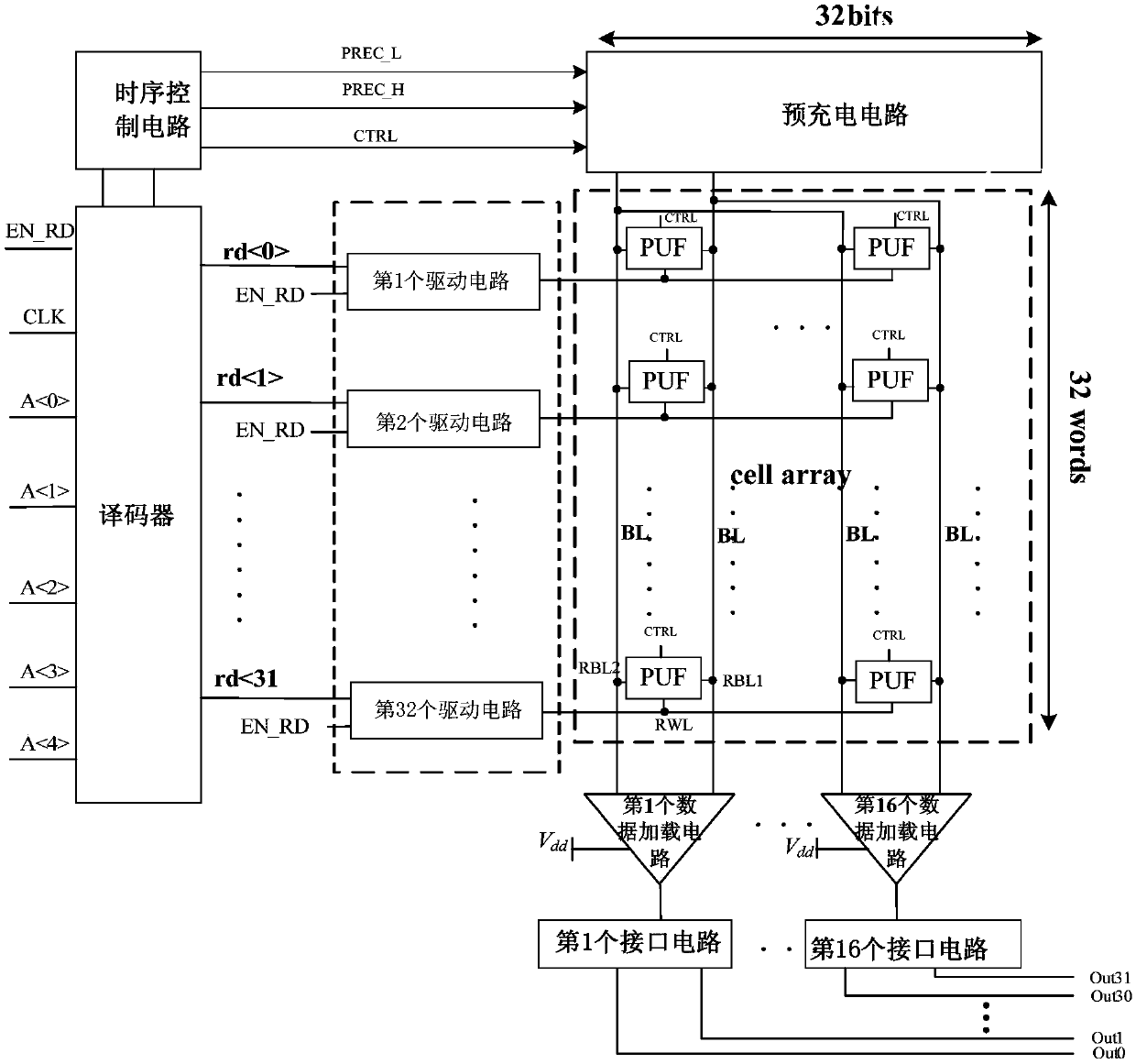
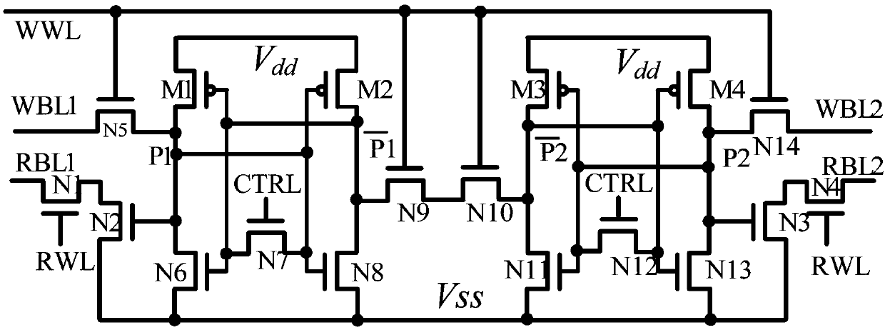
[0029] Embodiment one: if figure 1 As shown, a twin storage type multi-valued physical unclonable function circuit, including timing control circuit, decoder, driver, pre-charging circuit, PUF array, 16 data loading circuits and 16 interface circuits; the driver includes 32 The driving circuit with the same structure, the driving circuit has an enabling terminal, an input terminal and an output terminal; the PUF array is formed by 512 PUF circuits arranged in a manner of 32 rows x 16 columns, and the PUF circuit has a control terminal, an address selection terminal, and a first output terminal. terminal and the second output terminal; the address selection terminals of the 16 PUF circuits located in the jth row are connected and its connection terminal is the address selection terminal of the jth row of the PUF array, j=1, 2, 3, ..., 32, located in the first row The first output terminals of the 32 PUF circuits in the k column are connected and the connection terminals are the f...
Embodiment 2
[0030] Embodiment two: if figure 1 As shown, a twin storage type multi-valued physical unclonable function circuit, including timing control circuit, decoder, driver, pre-charging circuit, PUF array, 16 data loading circuits and 16 interface circuits; the driver includes 32 The driving circuit with the same structure, the driving circuit has an enabling terminal, an input terminal and an output terminal; the PUF array is formed by 512 PUF circuits arranged in a manner of 32 rows x 16 columns, and the PUF circuit has a control terminal, an address selection terminal, and a first output terminal. terminal and the second output terminal; the address selection terminals of the 16 PUF circuits located in the jth row are connected and its connection terminal is the address selection terminal of the jth row of the PUF array, j=1, 2, 3, ..., 32, located in the first row The first output terminals of the 32 PUF circuits in the k column are connected and the connection terminals are the...
PUM
 Abstract
Description
Claims
Application Information
 - Generate Ideas
- Intellectual Property
- Life Sciences
- Materials
- Tech Scout
- Unparalleled Data Quality
- Higher Quality Content
- 60% Fewer Hallucinations
Browse by: Latest US Patents, China's latest patents, Technical Efficacy Thesaurus, Application Domain, Technology Topic, Popular Technical Reports.
© 2025 PatSnap. All rights reserved.Legal|Privacy policy|Modern Slavery Act Transparency Statement|Sitemap|About US| Contact US: help@patsnap.com


