Wide-bandgap semiconductor lateral double-diffused field effect transistor with transverse and longitudinal electric field simultaneous optimization function

A lateral double diffusion, semiconductor technology, applied in the direction of semiconductor devices, circuits, electrical components, etc., can solve the problem of limited effect of lateral electric field optimization

Inactive Publication Date: 2018-01-23
XIDIAN UNIV
View PDF3 Cites 0 Cited by
  • Summary
  • Abstract
  • Description
  • Claims
  • Application Information

AI Technical Summary

Problems solved by technology

[0007] The above two schemes are actually optimized for the vertical electric field of the device, but the optimization effect for the horizontal electric field is very limited

Method used


Image

  • Wide-bandgap semiconductor lateral double-diffused field effect transistor with transverse and longitudinal electric field simultaneous optimization function
  • Wide-bandgap semiconductor lateral double-diffused field effect transistor with transverse and longitudinal electric field simultaneous optimization function
  • Wide-bandgap semiconductor lateral double-diffused field effect transistor with transverse and longitudinal electric field simultaneous optimization function

Examples


Embodiment Construction

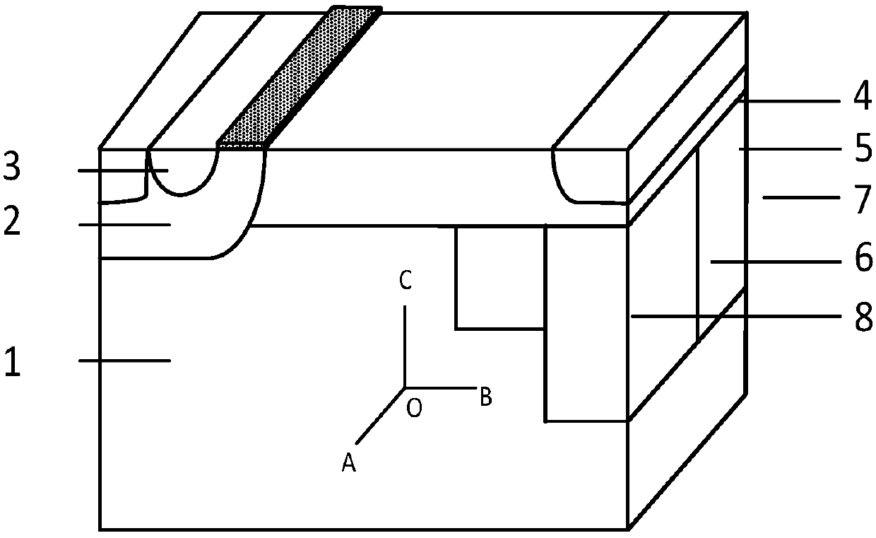
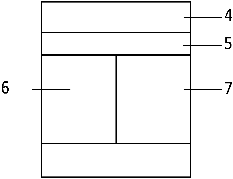
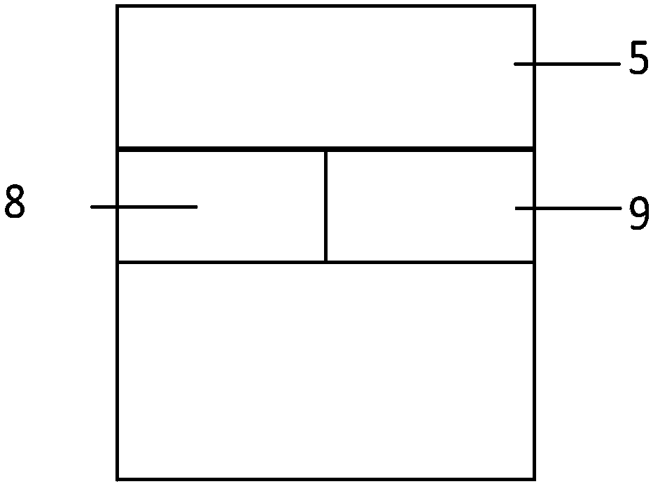
[0041] Such as figure 1 , figure 2 and image 3 Shown is a horizontal double-diffused transistor with horizontal and vertical electric fields and optimized wide bandgap semiconductor:

[0042] Wide bandgap semiconductor material substrate 1, the typical value of doping concentration is 1×10 13 cm -3 ~1×10 15 cm -3 ;

[0043] The base region 2 and the drift region 5 located on the surface of the substrate;

[0044] a source region 3 located on the surface of the base region;

[0045] a drain region 4 located on the surface of the drift region;

[0046] Under the drift region at the drain end are vertical auxiliary depletion substrate buried layers 6 and 7;

[0047] A portion of the charge compensation buried substrate 8, 9 is provided in the substrate region below the drift region and close to the auxiliary depleted buried substrate.

[0048] The vertical assisted depletion substrate buried layer can be N-type uniformly doped silicon material, P uniformly doped silicon...


PUM


Abstract

The invention discloses a wide-bandgap semiconductor lateral double-diffused field effect transistor with a transverse and longitudinal electric field simultaneous optimization function. An assisted depletion substrate buried layer is arranged below a drift region at the drain end, and a substrate buried layer with partial charge compensation is arranged in a substrate area below the drift regionof LDMOS and near the assisted depletion substrate buried layer. A new electric field peak is introduced to the surface transverse electric field of the device, so that the surface transverse electricfield of the device is distributed more uniformly, and the surface transverse electric field of the device is well optimized. A new electric field peak is also introduced to the inside longitudinal electric field distribution of the device, which further optimizes the inside longitudinal electric field. The structure breaks through the voltage saturation phenomenon caused by the limited longitudinal withstand voltage. Most importantly, the surface transverse electric field and the inside longitudinal electric field can be optimized simultaneously, and the breakdown voltage of the device is greatly improved.

Description

technical field [0001] The invention relates to the technical field of semiconductor power devices, in particular to a lateral double-diffusion transistor. Background technique [0002] Lateral Double-diffused MOSFET (LDMOS) has the advantages of easy integration, good thermal stability, good frequency stability, low power consumption, multi-subconduction, small power drive, and switching speed Advanced advantages are at the heart of smart power circuits and high-voltage devices. Due to the growing market demand for portable power management and automotive electronics, it is receiving increasing attention across the globe. [0003] However, due to the limitations of the first two generations of semiconductor materials represented by Si and GaAs, the third generation of wide-bandgap semiconductor materials has developed rapidly because of its excellent performance. Wide bandgap semiconductor materials have the characteristics of large bandgap width, high electron drift satu...

Claims


Application Information

Patent Timeline
Patent Type & Authority Applications(China)
IPC IPC(8): H01L29/78H01L29/06
Inventor 段宝兴董自明杨银堂
Owner XIDIAN UNIV
Why Eureka
Try Eureka