
Process for epitaxial growth of silicon in three-dimensional (3D) NAND flash structure

A technology of silicon epitaxy and flash memory, applied in the direction of electrical components, electrical solid devices, circuits, etc., can solve the increasingly difficult three-dimensional memory cleaning process, affect the performance of channel preparation 3D NAND flash memory, and affect the quality of silicon epitaxial growth, etc. problems, to achieve the effect of avoiding etching damage to the interface layer, eliminating interface damage and lattice defects, good oxidation annealing and interface repair

Inactive Publication Date: 2018-01-19
YANGTZE MEMORY TECH CO LTD
View PDF4 Cites 12 Cited by
  • Summary
  • Abstract
  • Description
  • Claims
  • Application Information

AI Technical Summary

Problems solved by technology

[0010] However, in the above process, as the number of stacked N / O (Nitride / Oxide) stacking structures in 3D NAND flash memory increases, it becomes more and more difficult to form through etching channels and subsequent cleaning processes in three-dimensional memories. bigger
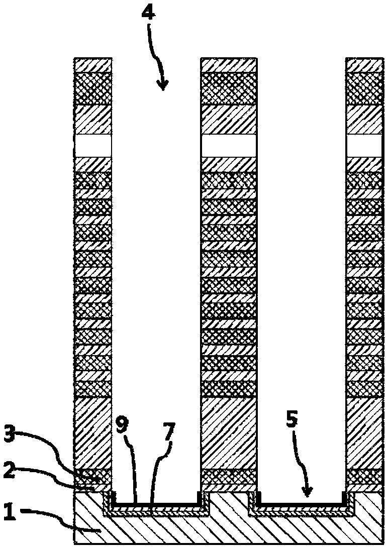
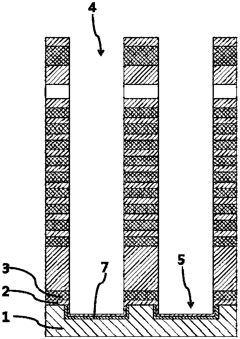
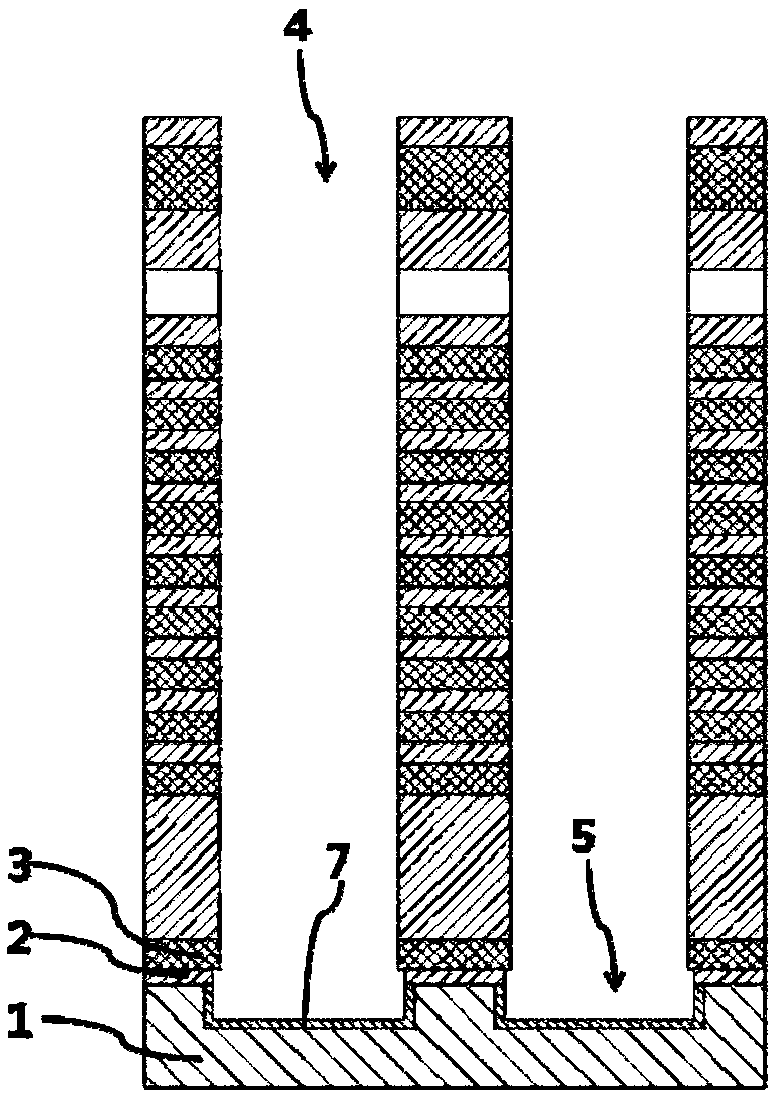
In order to effectively etch to form a channel, an etch damage layer 7 is often formed at the interface of the etched region (see Figure 1a ), and the interface damage and lattice defects of these etching damage layers will not be repaired in the subsequent pre-cleaning steps, which will further affect the quality of silicon epitaxial growth, such as causing the height of the silicon epitaxial layer to be uneven and vacancies8 (see Figure 1d ) generation
Not only that, but the deep trench also makes it difficult to effectively remove the residual polymer9 at the bottom of the etched trench (see Figure 1a ), which also affects the quality of silicon epitaxial growth
These problems will affect the preparation of the channel and the performance of the final 3D NAND flash memory

Method used


Image

  • Process for epitaxial growth of silicon in three-dimensional (3D) NAND flash structure
  • Process for epitaxial growth of silicon in three-dimensional (3D) NAND flash structure
  • Process for epitaxial growth of silicon in three-dimensional (3D) NAND flash structure

Examples


Embodiment Construction

[0036] Exemplary embodiments of the present disclosure will be described in more detail below with reference to the accompanying drawings. Although exemplary embodiments of the present disclosure are shown in the drawings, it should be understood that the present disclosure may be embodied in various forms and should not be limited by the embodiments set forth herein. Rather, these embodiments are provided for more thorough understanding of the present disclosure and to fully convey the scope of the present disclosure to those skilled in the art.

[0037] In the interest of clarity, not all features of an actual implementation are described. In the following description, well-known functions and constructions are not described in detail since they would obscure the invention with unnecessary detail. It should be appreciated that in the development of any actual embodiment, numerous implementation details must be worked out to achieve the developer's specific goals, such as ch...


PUM


Abstract

The invention provides a process for epitaxial growth of silicon in a three-dimensional (3D) NAND flash structure. The method comprises the steps of depositing a substrate lamination structure; etching the substrate lamination structure to form a channel and a silicon groove in a substrate surface; cleaning the channel and the silicon groove; performing high-temperature annealing; forming epitaxial growth of the silicon, and cleaning the silicon in advance; and performing epitaxial growth of the silicon. By high-temperature annealing, the surface of the silicon groove damaged by etching is oxidized, so that resided polymer in the silicon groove in the bottom of the channel is eliminated, meanwhile, a certain oxidization repair effect also can be generated on the surface, which is damaged,of the silicon subsequently and epitaxially grown, and interface damage and lattice defect are eliminated; the step of wet cleaning is added before high-temperature annealing, the subsequent and better effects of oxidization annealing and interface repair can be obtained; and by the process, the deep channel can be effectively etched, oxide residue is prevented, damage to an interface layer by etching is prevented, so that the epitaxial growth height uniformity of the silicon is improved, an epitaxial growth gap of the silicon is prevented, and the comprehensive performance of a 3D NAND flashis improved.

Description

technical field [0001] The invention relates to the field of semiconductor manufacturing, in particular to a 3D NAND flash memory structure and a manufacturing method thereof, in particular to a silicon epitaxial growth process in a 3D NAND flash memory structure capable of improving the growth quality of a silicon epitaxial layer. Background technique [0002] With the development of planar flash memory, the production process of semiconductors has made great progress. However, in recent years, the development of planar flash memory has encountered various challenges: physical limits, existing development technology limits, and storage electron density limits. In this context, in order to solve the difficulties encountered in planar flash memory and to seek lower production costs per unit storage unit, various three-dimensional (3D) flash memory structures have emerged, such as 3D NOR (3D or not) flash memory and 3D NAND (3D NAND) flash memory. [0003] Wherein, in the 3D...

Claims


Application Information

Patent Timeline
Patent Type & Authority Applications(China)
IPC IPC(8): H01L27/11524H10B41/35
Inventor 张坤刘藩东何佳杨要华吴林春夏志良霍宗亮
Owner YANGTZE MEMORY TECH CO LTD
Learn More