Metal grid structure and formation method thereof

A metal gate and gate technology, applied in the field of metal gate structure and its formation, can solve the problems of oxide layer erosion and device leakage of devices, reduce the risk of fluorine erosion, improve performance, and reduce the risk of fluorine residues Effect

Active Publication Date: 2018-01-09
YANGTZE MEMORY TECH CO LTD
View PDF5 Cites 0 Cited by
  • Summary
  • Abstract
  • Description
  • Claims
  • Application Information

AI Technical Summary

Problems solved by technology

Metal tungsten is generally through tungsten hexafluoride WF 6 with hydrogen H 2 Reduction for deposition, the fluoride in the reaction process may remain in the pores, resulting in a higher fluorine element in the tungsten film, too high a fluorine content will corrode the oxide layer of the device, and then cause device leakage

Method used


Image

  • Metal grid structure and formation method thereof
  • Metal grid structure and formation method thereof
  • Metal grid structure and formation method thereof

Examples


Embodiment Construction

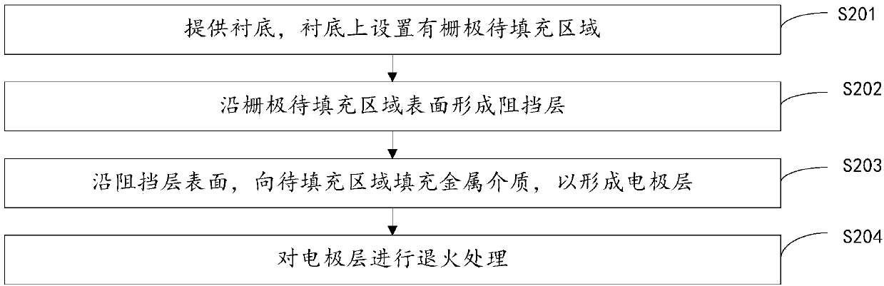
[0032] Embodiments of the present application are described below in conjunction with the accompanying drawings.

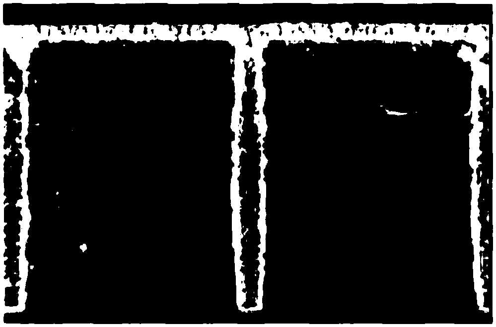
[0033] In the field of semiconductors, metal tungsten is often used to form metal gates due to its good resistance to electromigration and corrosion resistance. However, a gate formed by a chemical vapor deposition (Chemical Vapor Deposition) CVD process or an ALD process often has voids. The presence of such voids or voids greatly affects the performance of semiconductor devices.

[0034] The following is combined with the process of filling metal tungsten by CVD process to illustrate the principle of void generation and how voids affect device performance.

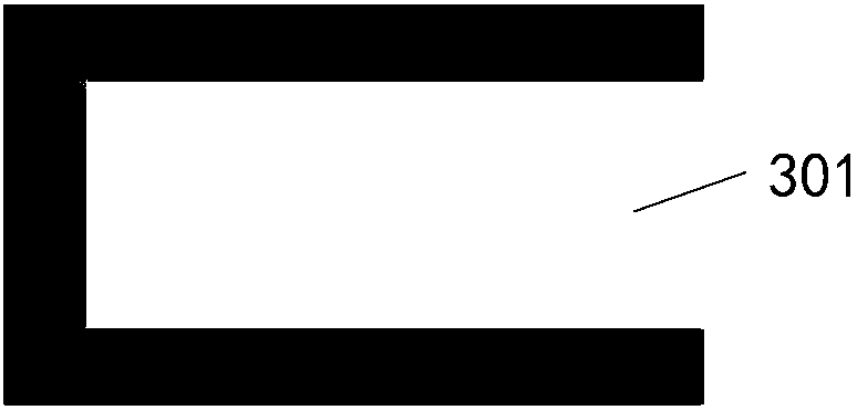
[0035] As the integration level of semiconductor devices becomes higher and higher, the feature size of the devices becomes smaller and smaller. The feature size can be understood as the line width of the integrated circuit, which is generally equal to the minimum width of the channel. The width of the ch...


PUM

PropertyMeasurementUnit
melting pointaaaaaaaaaa

Abstract

The embodiment of the invention discloses a metal grid formation method. The method comprises the steps of providing a substrate, wherein a grid region to be filled is arranged on the substrate; forming a blocking layer along a surface of the grid region to be filled; filling the region to be filled with a metal medium along a surface of the blocking layer to form an electrode layer; and annealingthe electrode layer so that metal atoms in the electrode layer can be automatically diffused. In the method, the diffusion activation energy of the metal atoms is relatively low, the metal atoms canbe automatically diffused after thermal treatment and can be diffused to holes with relatively high vacancy concentration, and the vacancy concentration can be balanced after the metal atoms are diffused to a certain extent; vacancies of hole positions are mostly occupied by the diffused metal atoms, and the holes are filled macroscopically; from an angle of a crystal, a grain boundary is migratedby migration of the atoms, the grain is grown, and the holes are also reduced; and since the holes are filled, the risk of fluorine residue is reduced, and the risk of fluorine corrosion is further reduced.

Description

technical field [0001] The present application relates to the field of semiconductors, in particular to a metal gate structure and a method for forming the same. Background technique [0002] With the development of information technology, the requirements for the computing speed and integration of semiconductor devices are gradually increased, and the feature size of semiconductor devices is gradually reduced. As a part of the device, the material of the gate greatly affects the performance of the device. Due to the "polysilicon depletion" effect in the traditional polysilicon gate process, which affects the conduction of the device, a metal gate is introduced. [0003] In metal gate technology, tungsten gate is widely used. As the filling aspect ratio becomes higher and higher, the step coverage of the filling process is challenged. During the growth process of metal tungsten, even if an atomic layer deposition (Atomic Layer Deposition, ALD) process is used, voids will ...

Claims


Application Information

Patent Timeline
Patent Type & Authority Applications(China)
IPC IPC(8): H01L21/28H01L21/283
Inventor 左明光彭浩万先进吴关平
Owner YANGTZE MEMORY TECH CO LTD
Why Eureka
Try Eureka