
A kind of LED chip cutting and splitting method

A technology of LED chips and chips, applied in the manufacture of semiconductor devices, electrical components, semiconductor/solid-state devices, etc., can solve the problems of warping of metal coils, residual metal residues, etc., so as to simplify the cutting process and improve the slicing yield. and product yield, the effect of solving the warping effect of metal coils

Active Publication Date: 2020-10-30
LATTICE POWER (JIANGXI) CORP
View PDF5 Cites 0 Cited by
  • Summary
  • Abstract
  • Description
  • Claims
  • Application Information

AI Technical Summary

Problems solved by technology

[0004] Based on the above problems, the object of the present invention is to provide a method for cutting and splitting LED chips, which effectively solves the problems of metal coil warping and residual metal residue caused by the existing splitting method.

Method used


Image

  • A kind of LED chip cutting and splitting method
  • A kind of LED chip cutting and splitting method
  • A kind of LED chip cutting and splitting method

Examples


Embodiment Construction

[0025] In order to make the technical problems, technical solutions and beneficial effects solved by the present invention clearer, the present invention will be further described in detail below in conjunction with the embodiments.

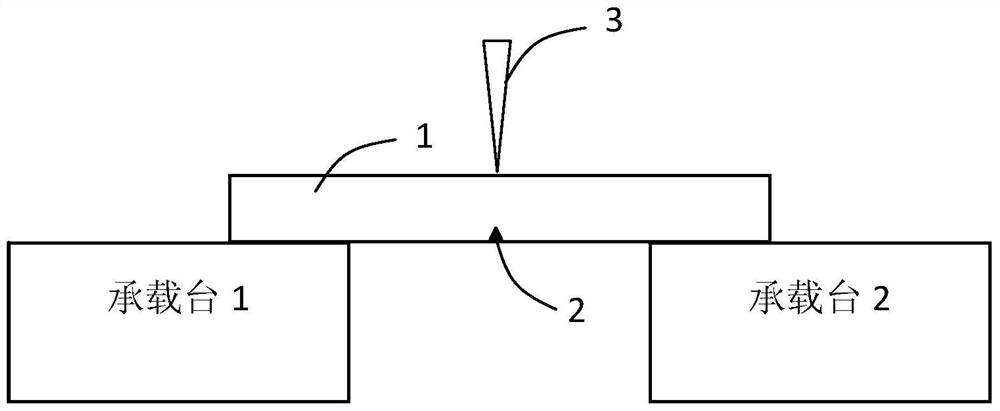
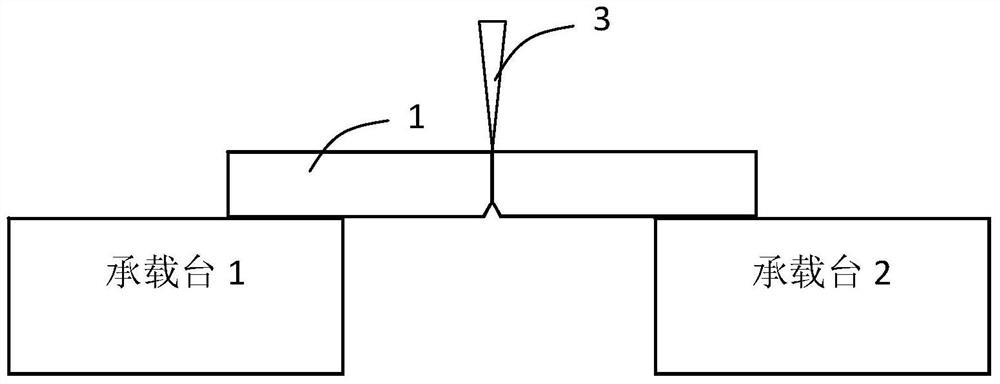
[0026] The invention provides a method for cutting and splitting an LED chip. Specifically, the cutting and splitting method is applied to an LED chip whose lower surface includes a metal layer on the back. The cutting and splitting method specifically includes: S1 on the upper surface of the LED chip Cut out grooves with a preset thickness; S2 splits along the lower surface of the LED chip to complete the complete splitting of the LED chip. It can be seen from the description that the upper surface of the LED chip is used for graphics and electrodes (light emitting), and the lower surface is evaporated for the back gold metal layer for eutectic soldering packaging, such as an Au-Sn alloy material layer with certain toughness.

[0027] More speci...


PUM


Abstract

The invention provides a method for cutting and splitting an LED chip, which specifically includes: S1 cutting a groove with a preset thickness on the upper surface of the LED chip; S2 splitting along the lower surface of the LED chip to complete the splitting of the LED chip Totally cleaved. After adopting the cutting and splitting method provided by the present invention, the cutting process flow is greatly simplified, and the problems caused by the existing cutting method such as warping of the metal coil and remaining metal residues are effectively solved.

Description

technical field [0001] The invention belongs to the field of semiconductors, and in particular relates to a method for cutting and splitting an LED chip. Background technique [0002] At present, conventional cutting and splitting methods of LED chips include laser cutting, blade cutting and other methods. Among them, in the laser cutting method, the laser is generally used to scribe the front and back surfaces of the LED chip before mechanical splitting; in the blade cutting method, the blade is generally used to cut a certain depth on the front and back surfaces of the LED chip before splitting. . [0003] Using the above method to cut and split the LED chip, although the production speed is high and the cost is low, but in some LED chips with metal back plating, due to the toughness of the metal, if the above conventional method is still used to cut and split it, It will bring a series of problems, such as warped metal rolls, residual metal residue, etc. However, it is...

Claims


Application Information

Patent Timeline
Patent Type & Authority Patents(China)
IPC IPC(8): H01L33/00H01L21/78
Inventor 邝耘丰杨杰封波龚文明
Owner LATTICE POWER (JIANGXI) CORP
Learn More