SiC ohmic contact structure and fabrication method thereof
A manufacturing method, ohmic contact technology, applied in the manufacture of semiconductor/solid-state devices, electrical components, circuits, etc., can solve the problems of reduced reliability of ohmic contact electrodes, limited application environment and range, and limitations, so as to achieve good I-V characteristics and improve Effect of Thermal Stability and Antioxidant Properties
- Summary
- Abstract
- Description
- Claims
- Application Information
AI Technical Summary
Problems solved by technology
Method used
Image
Examples
Embodiment 1
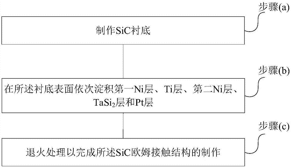
[0040] See figure 1 , figure 1 A SiC ohmic contact process flow chart provided for an embodiment of the present invention, including:
[0041] (a) making a SiC substrate;
[0042] (b) sequentially depositing a first Ni layer, a Ti layer, a second Ni layer, TaSi on the substrate surface 2 layer and Pt layer;
[0043] (c) performing a first annealing treatment to complete the fabrication of the SiC ohmic contact structure.
[0044] Preferably, step (a) may include:
[0045] (a1) selecting a 4H-SiC substrate and performing standard RCA cleaning on the 4H-SiC substrate;
[0046] (a2) Depositing an oxide layer with a thickness of 100 nm on the surface of the 4H-SiC substrate by PECVD process;
[0047] (a3) Etching the oxide layer to form an ion implantation window, and performing N on the surface of the 4H-SiC substrate by using an ion implantation process + ,P + Ion implantation forms N-type doped regions and P-type doped regions;
[0048] (a4) Etching away the remaining ...
Embodiment 2
[0065] The present invention proposes a kind of utilization Pt / TaSi 2 / Ni / Ti / Ni / SiC structure method for making SiC ohmic contacts, including:
[0066] S201, select a 4H-SiC substrate, and perform standard RCA cleaning on the 4H-SiC substrate;
[0067] S202, using the PECVD process, deposit SiO with a thickness of 100nm on the 4H-SiC substrate 2 oxide layer;
[0068] S203, etching the oxide layer to form an ion implantation window, for 4H-SiC substrate N + or P + Ion implantation to form highly doped N or P regions and perform high temperature annealing;
[0069] S204, etching the remaining oxide layer;
[0070] S205, depositing a metal layer on the 4H-SiC substrate, the metal layer sequentially includes a first Ni layer, a Ti layer, a second Ni layer, TaSi 2 layer and Pt layer;
[0071] S206 , rapid annealing to form an ohmic contact.
[0072] Preferably, the doping source of the N-type doping region in step S203 is Al, and the doping concentration is 1.0×10 20 cm -...
Embodiment 3
[0090] Please refer to Figure 9 , Figure 9 A cross-sectional view of a SiC ohmic contact structure provided for an embodiment of the present invention; the SiC ohmic contact structure includes: a SiC substrate 1, and a first Ni layer 2, a Ti layer 3, and a second Ni layer arranged on the SiC substrate in sequence. Ni layer 4, TaSi 2 Layer 5 and Pt layer 6.
PUM
| Property | Measurement | Unit |
|---|---|---|
| Thickness | aaaaa | aaaaa |
| Thickness | aaaaa | aaaaa |
| Thickness | aaaaa | aaaaa |
Abstract
Description
Claims
Application Information
 - R&D
- Intellectual Property
- Life Sciences
- Materials
- Tech Scout
- Unparalleled Data Quality
- Higher Quality Content
- 60% Fewer Hallucinations
Browse by: Latest US Patents, China's latest patents, Technical Efficacy Thesaurus, Application Domain, Technology Topic, Popular Technical Reports.
© 2025 PatSnap. All rights reserved.Legal|Privacy policy|Modern Slavery Act Transparency Statement|Sitemap|About US| Contact US: help@patsnap.com


