
Shield gate trench MOSFET and manufacture method

A manufacturing method and shielding gate technology, which is applied in semiconductor/solid-state device manufacturing, electrical components, circuits, etc., can solve problems such as limited device use, low on-resistance, and large gate-to-drain capacitance, so as to improve switching speed and reduce grid Leakage capacitance, the effect of improving the degree of integration

Active Publication Date: 2017-12-29
SHANGHAI HUAHONG GRACE SEMICON MFG CORP
View PDF5 Cites 22 Cited by
  • Summary
  • Abstract
  • Description
  • Claims
  • Application Information

AI Technical Summary

Problems solved by technology

[0020] like Figure 1I The existing shielded gate trench MOSFET shown has the advantage of low on-resistance. When the device is turned on, all channels are turned on, and its gate-to-drain capacitance is large, which limits the use of the device in high switching speed applications.
How to reduce the gate charge of the device to reduce the gate-to-drain capacitance becomes a challenge in process and design

Method used


Image

  • Shield gate trench MOSFET and manufacture method
  • Shield gate trench MOSFET and manufacture method
  • Shield gate trench MOSFET and manufacture method

Examples


Embodiment Construction

[0066] Such as figure 2 As shown, it is a schematic diagram of the device structure of the embodiment of the present invention; the gate structure of the shielded gate trench MOSFET of the embodiment of the present invention includes:

[0067] A gate trench formed in the semiconductor substrate 1, the gate trench includes a top trench 301 and a bottom trench 302, the width of the bottom trench 302 is defined by a photolithography process, and the top trench 301 The width of is added to the width formed by isotropic etching on the basis of the definition of the photolithography process. In the embodiment of the present invention, a first epitaxial layer of the first conductivity type is formed on the surface of the semiconductor substrate 1 , and the gate trench is located in the first epitaxial layer.

[0068] A gate dielectric layer 2 and a polysilicon gate 3 are respectively formed in the regions formed by isotropic etching on both sides of the top trench 301; The bottom ...


PUM


Abstract

The invention discloses a shield gate trench MOSFET. The gate trench includes a top trench and a bottom trench. A polysilicon gate is formed on both sides of the top trench. Source polysilicon is located in the middle of the gate trench and extends longitudinally through the entire gate trench. Channel regions are formed on semiconductor substrate surfaces between gate structures and source regions are formed on the surfaces of the channel regions. A polysilicon gate on one side of the top trench is connected to a gate formed by a front metal layer. A polysilicon gate on the other side of the top trench and the source regions are connected to a source through a second contact hole to form a structure for reducing the gate-drain capacitance of a device. The second contact hole reduces the distance between the gate trenches and reduces the on-resistance of the device and form an on-resistance compensation structure. The invention also discloses a method for manufacturing the shield gate trench MOSFET. The shield gate trench MOSFET can reduce the gate-drain capacitance, can increase the switching speed of the device, and can reduce the size of a unit device and improve an integration level.

Description

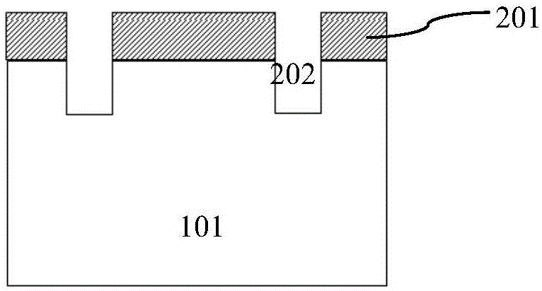
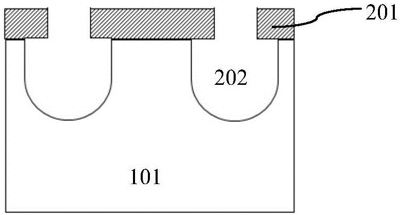
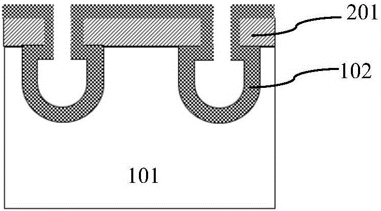
technical field [0001] The invention relates to the field of semiconductor integrated circuit manufacturing, in particular to a shield gate (Shield Gate Trench, SGT) trench MOSFET; the invention also relates to a manufacturing method of the shield gate trench MOSFET. Background technique [0002] Such as Figure 1A to Figure 1I Shown is a schematic diagram of the device structure in each step of the existing method; the manufacturing method of the existing shielded gate trench MOSFET includes the following steps: [0003] Step 1, such as Figure 1A As shown, a semiconductor substrate such as a silicon substrate 101 is provided, and a formation region of a gate trench is defined by a photolithography process, and the gate trench includes a plurality of gate trenches. [0004] The step of forming a hard mask layer 201 on the surface of the semiconductor substrate 101 is included before the photolithography process, and the hard mask layer 201 is etched and formed after the fo...

Claims


Application Information

Patent Timeline
Patent Type & Authority Applications(China)
IPC IPC(8): H01L29/423H01L29/78H01L21/336H01L21/28
CPCH01L29/4236H01L29/66484H01L29/66666H01L29/7827H01L29/7831
Inventor 范让萱缪进征
Owner SHANGHAI HUAHONG GRACE SEMICON MFG CORP
Learn More