A Method for Calculating the Area of ​​Combined Figures in Electronic Layout

A technology combining graphics and electronic versions, applied in computing, computer-aided design, electronic digital data processing, etc., can solve the problems of easy omission or repeated calculation of calculation results, complicated calculation, inaccurate calculation, etc., to shorten the calculation time, application Wide-ranging, accurately calculated effects

Active Publication Date: 2020-07-28
NORTH ELECTRON RES INST ANHUI CO LTD
View PDF2 Cites 0 Cited by
  • Summary
  • Abstract
  • Description
  • Claims
  • Application Information

AI Technical Summary

Problems solved by technology

[0010] However, electronic layout usually uses special design software such as Protel, Cadence, Powerpcb, etc. These software do not have the function of area calculation, as shown in the attached figure 1 As shown, if you want to use special design software such as Protel to calculate the area, the existing technology can be obtained by measuring the length and width of each figure, calculating the area and then accumulating to obtain it. There is also superposition between the graphics, and there may be a round corner transition at the superposition. The existing calculation cannot take this factor into account, and it also affects the accuracy of the calculation results. Therefore, the existing technology is time-consuming and labor-intensive, and the calculation is inaccurate
For the area of ​​slightly more complex graphics, this method needs at least 1 day to measure and calculate one by one, and it also needs repeated proofreading

Method used


Image

  • A Method for Calculating the Area of ​​Combined Figures in Electronic Layout
  • A Method for Calculating the Area of ​​Combined Figures in Electronic Layout
  • A Method for Calculating the Area of ​​Combined Figures in Electronic Layout

Examples


Embodiment Construction

[0044] The invention provides a method for calculating the area of ​​combined graphics of an electronic layout, comprising the following steps:

[0045] Step a, export the electronic layout as a GBR file in the EDA software for making the electronic layout;

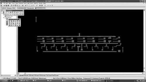
[0046] This embodiment takes PROTEL software as an example for specific description, such as figure 1 Shown is a gold conduction band single-layer printed pattern electronically laid out in the Protel environment.

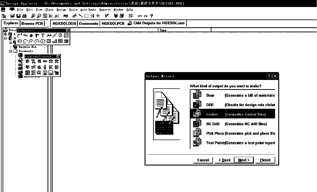
[0047] combine figure 2 As shown, enter Protel, open the PCB file, click File→CAM Manager in turn, in figure 2 Click "NEXT" in the pop-up menu, see the pop-up menu image 3 ,exist image 3 Select "Gerber" in the pop-up menu and then click "NEXT" continuously. When entering the graphics unit selection interface, generally select inch. When entering the layer selection interface, select the outer frame layer and the layer to be calculated. Continue to click "NEXT" continuously, and finally click "Finish"....


PUM


Abstract

The invention discloses a method for calculating a composite graph area of an electronic layout. The method comprises the steps that the electronic layout is exported to be a GBR file in EDA software used for making the electronic layout; the GBR file is imported into CAM350 software; merging processing is performed on a border layer and a printing layer of the imported electronic layout file in the CAM350 software; a gap between the border layer and the printing layer of the file processed in the step c is filled up in the CAM350 software; a background layer and a filling layer of the file processed in the step d are separated in the CAM350 software; the file processed through the CAM350 software is exported to be a dxf file; the dxf file is imported into AUTOCAD software, and regions are created for the imported file in the AUTOCAD software; the regions are merged in the AUTOCAD software; and the AUTOCAD software is utilized to calculate the border area S1 and the area S2 of a region obtained after merging, and the composite graph area S of the electronic layout is obtained by subtracting S2 from S1. Through the method, calculation of the total area of a composite graph obtained after combination is realized; and printing area calculation efficiency is high, and calculation time can be substantially shortened.

Description

technical field [0001] The invention relates to the technical field of microelectronics manufacturing, in particular to a method for calculating the combined graphic area of ​​an electronic layout. Background technique [0002] Thick-film hybrid integrated circuits or PCB printed circuit boards and other electronic products need to be drawn in advance in the electronic design software, and the graphics of the specific lines in the layout file are then printed on the substrate materials such as ceramics and PCBs by means of light drawing and plate making. Print or deposit other metal materials on the upper layer, and the printed or deposited graphics should be consistent with the design graphics. [0003] In actual production, due to the high cost of materials, especially when the printing materials are gold-containing materials, because the gold-containing materials are expensive, they need to be purchased. However, this type of material costs several hundred yuan per gram o...

Claims


Application Information

Patent Timeline
Patent Type & Authority Patents(China)
IPC IPC(8): G06F30/392
CPCG06F30/392
Inventor 李寿胜尤广为臧子昂钱晓晴
Owner NORTH ELECTRON RES INST ANHUI CO LTD
Why Eureka
Try Eureka