A kind of circuit board and optical module

A circuit board and optical module technology, applied in the field of optical communication, can solve problems such as poor working stability, and achieve the effects of improving performance, reducing interference current, and reducing the impact of withstand programs

Active Publication Date: 2019-12-20
HISENSE BROADBAND MULTIMEDIA TECH
View PDF9 Cites 0 Cited by
  • Summary
  • Abstract
  • Description
  • Claims
  • Application Information

AI Technical Summary

Problems solved by technology

[0010] The purpose of the embodiment of the present invention is to provide a circuit board and an optical module, which is used to solve the problem of poor working stability of the CDR circuit of the laser driver chip in the harsh low temperature environment in the existing optical module

Method used


Image

  • A kind of circuit board and optical module
  • A kind of circuit board and optical module
  • A kind of circuit board and optical module

Examples


Embodiment Construction

[0033] A circuit board and an optical module provided by the present invention will be described in more detail below with reference to the drawings and embodiments.

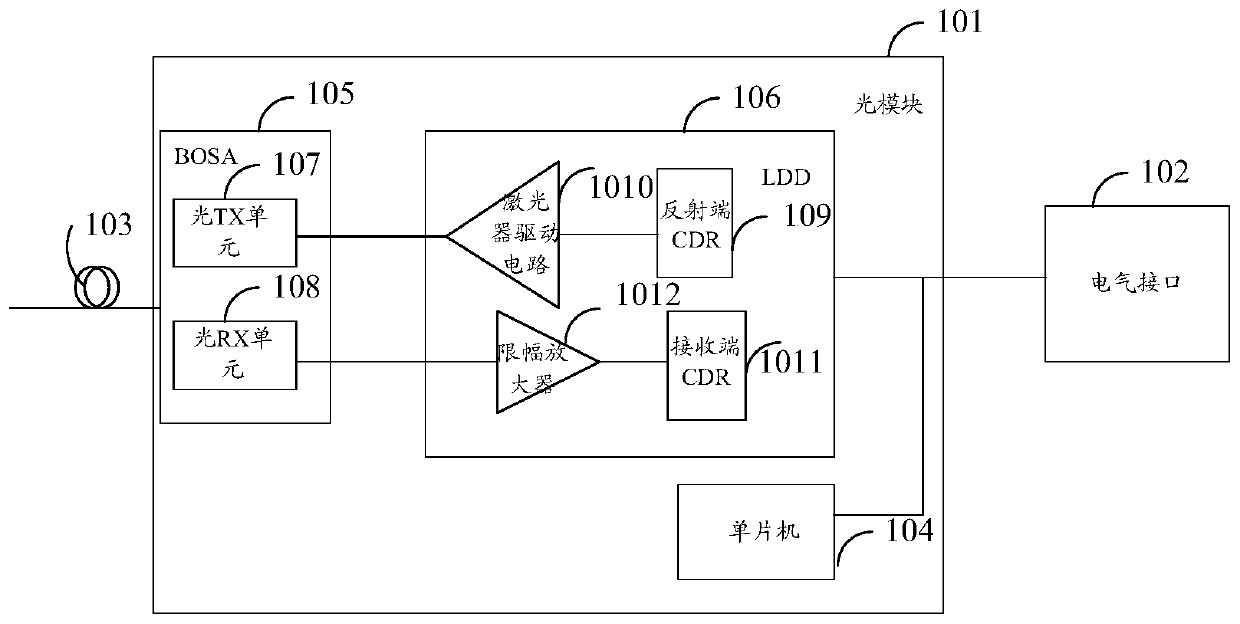
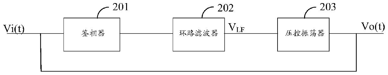
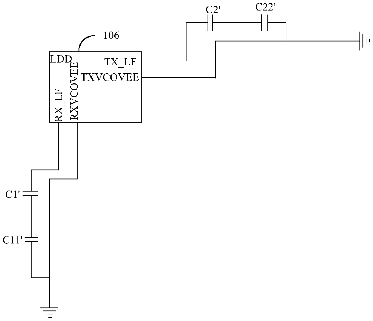
[0034] Such as Figure 5a and Figure 5b As shown, the embodiment of the present invention provides a circuit board, which is applied in an optical module. The circuit board 501 is provided with a laser driver chip 502 and a filter capacitor unit 503; wherein, the laser driver chip 502 has a CDR circuit; the CDR circuit has a frequency-locked pin 504 and reference ground pin 505; the circuit board is also provided with laminated ground layer 506, insulating layer 507 and wiring layer; wherein, one end of the filter capacitor unit 503 is connected to the frequency-locked circuit through the first wiring 508 of the wiring layer The pin 504 is connected, and the other end is connected to the reference ground pin 505 through the second wiring 509 of the wiring layer; wherein:

[0035] A node on the second trace 50...


PUM


Abstract

The embodiment of the invention discloses a circuit board and an optical module. The circuit board in this scheme is applied in the optical module, and the laser driver chip and filter capacitor unit are arranged on the circuit board; wherein, the laser driver chip has a CDR circuit; the CDR circuit has a frequency locking pin and a reference ground pin; the circuit board is also provided with a stacked ground layer, an insulating layer and a wiring layer; wherein, one end of the filter capacitor unit passes through the first wiring of the wiring layer and the frequency-locking pin The other end is connected to the reference ground pin through the second trace of the trace layer; wherein: a node on the second trace is connected to the ground layer through a via hole, so that the filter capacitor The cell and reference ground pins are connected to ground. In the existing optical module, the problem of poor working stability of the CDR circuit of the laser driver chip under extreme conditions is solved.

Description

technical field [0001] The invention relates to the technical field of optical communication, in particular to a circuit board and an optical module. Background technique [0002] In optical communication, the optical module can realize photoelectric conversion. With the rapid development of the optical communication industry, the transmission rate and distance of the communication network have increased significantly, and the dispersion and link attenuation have become more serious. High requirements, using a laser driver chip with clock and data recovery (Clock and data recovery, CDR) function, can realize clock recovery extraction, so that the distorted signal can be recovered, improve the signal quality, improve the sensitivity of signal recognition, and increase the link margin to improve robustness. [0003] The CDR technology integrated in the laser driver chip of the optical module is relatively mature, see figure 1 As shown in the optical module 101, one end of th...

Claims


Application Information

Patent Timeline
Patent Type & Authority Patents(China)
IPC IPC(8): H05K1/02
CPCH05K1/0216H05K2201/09672
Inventor 董淑芬谭祖炜朱德锋薛开锋
Owner HISENSE BROADBAND MULTIMEDIA TECH
Why Eureka
Try Eureka