Substrate leveling equipment and semiconductor fabrication method employing same

A manufacturing method and semiconductor technology, applied in semiconductor/solid-state device manufacturing, electrical components, circuits, etc., can solve problems such as substrate deformation, substrate clamping and fixing, and substrate warpage

Active Publication Date: 2017-12-08
GRAND PLASTIC TECH
View PDF14 Cites 2 Cited by
  • Summary
  • Abstract
  • Description
  • Claims
  • Application Information

AI Technical Summary

Problems solved by technology

[0003] However, when the substrate passes through the above multiple grinding, machining and high temperature processes, the substrate will be deformed due to the influence of mechanical force or thermal stress
Especially for thin substrates (such as silicon wafers or glass substrates, etc.), after various processing and high-temperature processes, it is more likely to cause severe deformation of the substrate and cause the substrate to show irregular warpage as a whole.
Therefore, when the warped substrate is undergoing processes such as cleaning or etching, the substrate is not placed flatly on the rotary chuck, thus causing the rotary chuck to fail to smoothly vacuum absorb the substrate through the vacuum chuck to fix it on it.
Or due to the structural interference between the warped edge of the substrate and the jaws of the rotary chuck, the jaws cannot smoothly clamp and fix the substrate on the rotary chuck

Method used


Image

  • Substrate leveling equipment and semiconductor fabrication method employing same
  • Substrate leveling equipment and semiconductor fabrication method employing same
  • Substrate leveling equipment and semiconductor fabrication method employing same

Examples


Embodiment Construction

[0022] In order to make the above and other objects, features, and advantages of the present invention more comprehensible, preferred embodiments of the present invention will be exemplified below in detail with accompanying drawings.

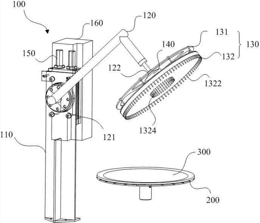
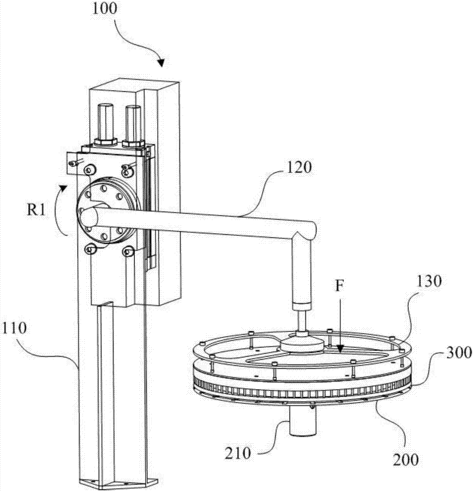
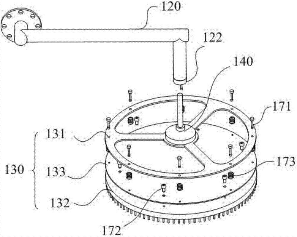
[0023] Please refer to figure 1 , which shows a schematic perspective view of a substrate flattening device 100 according to the first preferred embodiment of the present invention. The substrate flattening apparatus 100 includes a base 110 , a rotating arm 120 and a disc assembly 130 . One end of the base 110 can be fixed on the ground or erected on a transport mechanism, and the substrate flattening device 100 can be transported to a working position through the transport mechanism. Such as figure 1 As shown, the rotating arm 120 is roughly in an "L" shape and has a first end 121 and a second end 122 . The first end 121 of the rotating arm 120 is rotatably connected to the base 110 through a rotating power device 150 , and the second end 1...


PUM


Abstract

The invention provides substrate leveling equipment and a semiconductor fabrication method employing the same. The substrate leveling equipment comprises a base, a rotation arm and a disc-shaped assembly, wherein one end of the rotation arm is rotatably connected with the base, the disc-shaped assembly is connected with the other end of the rotation arm, the disc-shaped assembly moves downwards with the rotation of the rotation arm on a vertical plane so that a disc surface of the disc-shaped assembly is laminated and supported on a substrate of a rotation clamping head, and vertical and downward pressure is applied to the substrate so that the substrate is smoothly laminated on the rotation clamping head.

Description

technical field [0001] The invention relates to a substrate flattening device, in particular to a substrate flattening device used in a semiconductor process. Background technique [0002] With the advancement of technology, electronic devices are developing towards miniaturization and precision, which makes the process of semiconductors more complicated. For example, semiconductor substrates need to undergo multiple processes such as grinding, machining, etching, and high-temperature heating to form integrated circuits in electronic devices. In addition, when the substrate is undergoing processes such as cleaning or etching, the substrate is generally fixed on a spin chuck by vacuum adsorption or edge clamping, and the substrate is rotated at a high speed and sprayed on top for cleaning or Etching liquid. [0003] However, after the substrate passes through the above multiple grinding, machining and high temperature processes, the substrate will be deformed due to the inf...

Claims


Application Information

Patent Timeline
Patent Type & Authority Applications(China)
IPC IPC(8): H01L21/67
CPCH01L21/67092
Inventor 黄富源刘文明陈薇云陈建龙
Owner GRAND PLASTIC TECH
Why Eureka
Try Eureka