Anisotropic conductive tape, tape roll, binding structure and display device
A conductive tape and anisotropic technology, used in conductors, circuits, adhesives, etc., can solve the problems of a small number of conductive contact balls, abnormal module display, poor signal conduction, etc., to improve product yield, Improve the uniformity of number and reduce the effect of poor binding process
- Summary
- Abstract
- Description
- Claims
- Application Information
AI Technical Summary
Problems solved by technology
Method used
Image
Examples
Embodiment 1
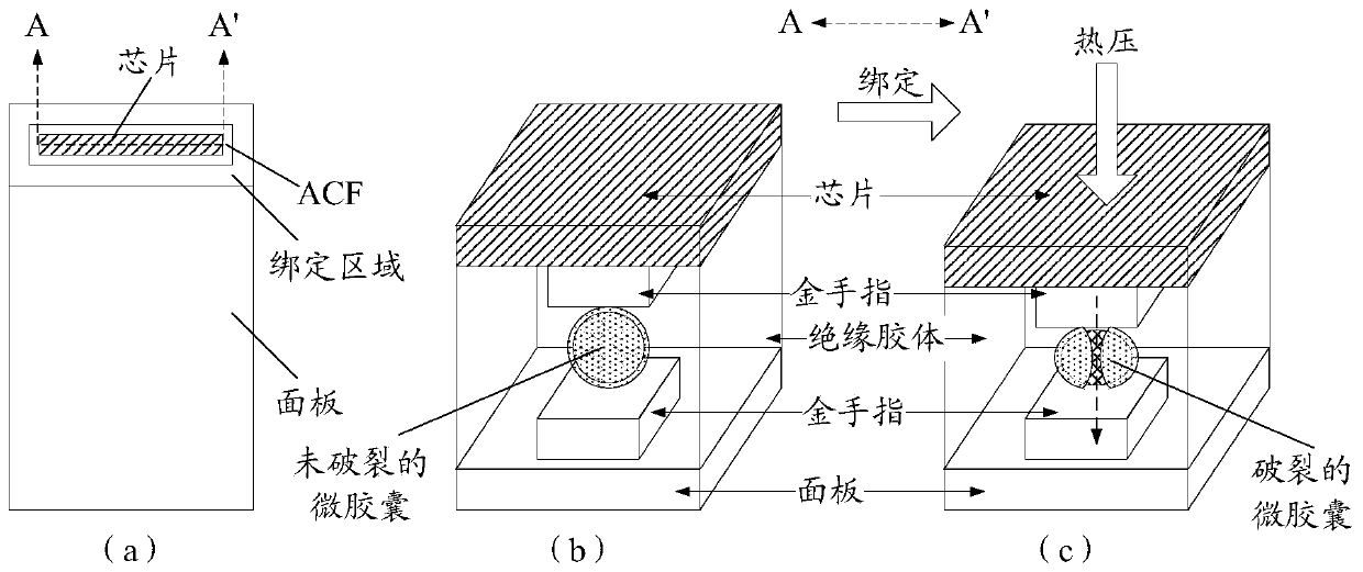
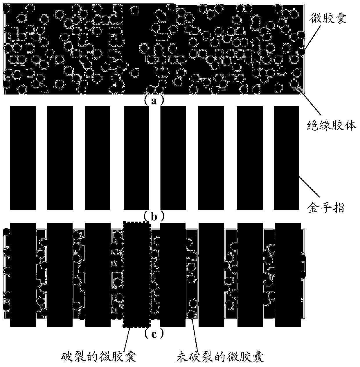
[0031] Such as image 3 As shown, the embodiment of the present invention provides an anisotropic conductive adhesive tape 1, the anisotropic conductive adhesive tape 1 includes an insulating adhesive layer 10, and the insulating adhesive layer 10 includes a plurality of spaced apart electrodes to be bound Corresponding preset area 10a (shown in dotted line frame among the figure); Capsule structure 11 dispersed in the insulating glue layer 10 of preset area 10a; This capsule structure 11 is used for being subjected to vertical When the pressure is applied in the direction of the tape surface, the conductive connection perpendicular to the direction of the tape surface is realized; wherein, the number of capsule structures 11 in each preset area 10a is greater than the preset number.
[0032] It should be noted that, first, the specific structures of the insulating adhesive layer 10 and the capsule structure 11 described above may follow the existing technology, which is not l...
Embodiment 2
[0048] The embodiment of the present invention also provides an anisotropic conductive tape roll. image 3 Anisotropic conductive tape 1 shown.
[0049] In this way, the roll of anisotropic conductive tape can be cut to form a reference in actual mass production figure 1 A single cut sheet is shown instead of the traditional ACF rolls in the prior art for binding process.
Embodiment 3
[0051] The embodiment of the present invention also provides a binding structure, which includes a first substrate and a second substrate oppositely arranged; wherein, a plurality of spaced apart first substrates are provided on the side of the first substrate facing the second substrate. An electrode (i.e. a raised binding structure, Bump), the second substrate is provided with a second electrode (i.e. a raised binding structure, Bump) vertically corresponding to the first electrode on the side facing the first substrate; Reference between a substrate and a second substrate image 3 The anisotropic conductive adhesive tape 1 shown; wherein, the above-mentioned predetermined area is located in the area vertically corresponding to the first electrode and the second electrode.
[0052] In this way, when the above-mentioned anisotropic conductive tape 1 is subjected to pressure perpendicular to the direction of the tape surface, the capsule structure 11 located in the predetermin...
PUM
 Abstract
Description
Claims
Application Information
 - Generate Ideas
- Intellectual Property
- Life Sciences
- Materials
- Tech Scout
- Unparalleled Data Quality
- Higher Quality Content
- 60% Fewer Hallucinations
Browse by: Latest US Patents, China's latest patents, Technical Efficacy Thesaurus, Application Domain, Technology Topic, Popular Technical Reports.
© 2025 PatSnap. All rights reserved.Legal|Privacy policy|Modern Slavery Act Transparency Statement|Sitemap|About US| Contact US: help@patsnap.com


