Piezoelectric film and preparation method thereof
A piezoelectric film and film-forming agent technology, applied in the manufacture/assembly of piezoelectric/electrostrictive devices, circuits, piezoelectric/electrostrictive/magnetostrictive devices, etc., can solve the problem of not being able to obtain large-area piezoelectric Thick films and piezoelectric thick films cannot be applied on a large scale to MEMS micro-drivers and a large number of cracks in piezoelectric films to achieve the effects of reducing cracks, improving mechanical properties, and surface integrity
- Summary
- Abstract
- Description
- Claims
- Application Information
AI Technical Summary
Problems solved by technology
Method used
Image
Examples
Embodiment 1
[0032] This embodiment discloses a piezoelectric film and a preparation method thereof. The material of the piezoelectric film is Pb(Zr 0.53 Ti 0.47 )O 3 and, the piezoelectric film has a thickness of 2 μm and an area of 4 inches, which greatly increases the area of the existing piezoelectric film, so compared to the piezoelectric film of the prior art, the purpose of this embodiment is to prepare a A large-area lead zirconate titanate piezoelectric "thick" film, referred to as PZT piezoelectric thick film.
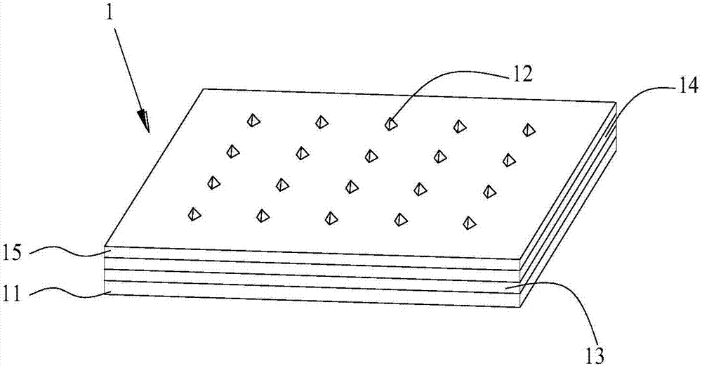
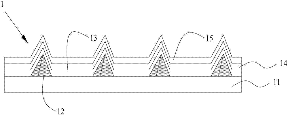
[0033] The piezoelectric film disclosed in this embodiment includes a substrate and a PZT piezoelectric film layer on the substrate. Specifically, refer to figure 1 and figure 2 , in this embodiment, the substrate 1 includes a base 11, a plurality of protrusions 12 arranged on the base 11, and an isolation layer 13, an electrode layer 14, and a crystal layer sequentially stacked on the base 11 and the protrusions 12. Seed layer 15.
[0034] More specifically, i...
Embodiment 2
[0053] In the description of Embodiment 2, the similarities with Embodiment 1 will not be repeated here, and only the differences with Embodiment 1 will be described. The difference between embodiment 2 and embodiment 1 is that the piezoelectric film of this embodiment is a ZnO piezoelectric thick film with a thickness of 5 μm, and the structure of the substrate and the shape of the protrusions are also different.
[0054] refer to Figure 4 and Figure 5 , in this embodiment, the substrate 2 includes a base 21 , a plurality of protrusions 22 disposed on the base 21 , and an isolation layer 23 and an electrode layer 24 sequentially stacked on the base 21 and the protrusions 22 .
[0055] Specifically, in this embodiment, the shape of the protrusions 22 is a sphere, and the arrays are arranged on the surface of the base 21 . The height of the spherical protrusion 22 in this embodiment is 12 μm, and its projected area on the surface of the base 21 is 314 μm 2 .
[0056] The ...
Embodiment 3
[0067] In the description of Embodiment 3, the similarities with Embodiment 1 will not be repeated here, and only the differences with Embodiment 1 will be described. The difference between Example 3 and Example 1 is that the piezoelectric film of this example is a PZT piezoelectric thick film with a thickness of 1.35 μm; at the same time, in the preparation method of this example, the steady-state liquid The film formers in the phase precursors are different.
[0068] Specifically, in this embodiment, the film-forming agent is 0.5g polyvinylpyrrolidone; The ratio is about 0.03:100.
[0069] In step three, repeat the operations of coating and preliminary annealing n times, in this embodiment, n is preferably 20; finally, sinter the 21-layer PZT piezoelectric film at 550°C-700°C for 5min-60min , preferably sintered at 700°C for 15 minutes for crystallization annealing.
[0070] For the rest, referring to the description in Example 1, a PZT piezoelectric thick film with a thi...
PUM
| Property | Measurement | Unit |
|---|---|---|
| Thickness | aaaaa | aaaaa |
| Thickness | aaaaa | aaaaa |
| Remanent polarization | aaaaa | aaaaa |
Abstract
Description
Claims
Application Information
 - R&D Engineer
- R&D Manager
- IP Professional
- Industry Leading Data Capabilities
- Powerful AI technology
- Patent DNA Extraction
Browse by: Latest US Patents, China's latest patents, Technical Efficacy Thesaurus, Application Domain, Technology Topic, Popular Technical Reports.
© 2024 PatSnap. All rights reserved.Legal|Privacy policy|Modern Slavery Act Transparency Statement|Sitemap|About US| Contact US: help@patsnap.com


