
Package structure

A packaging structure, epoxy resin technology, applied in electrical components, electrical solid devices, circuits, etc., can solve the problems of high price, complicated steps, high cost, avoid delamination, simplify the production process, and improve the bonding force.

Inactive Publication Date: 2017-10-31
IBIS INNOTECH
View PDF5 Cites 0 Cited by
  • Summary
  • Abstract
  • Description
  • Claims
  • Application Information

AI Technical Summary

Problems solved by technology

However, the steps of this process are complicated, and the cost of the sputtering process is relatively high
In addition, the patterned circuit layer formed by using the patterned dry film layer as a plating barrier is difficult to meet the current demand for fine pitch.
Furthermore, the insulating substrate is mostly made of polyimide or ABF (Ajinomoto build-up film) resin, which is relatively expensive.
Therefore, the current manufacturing of packaging substrates is not only complicated, but also costly

Method used


Image

  • Package structure
  • Package structure
  • Package structure

Examples


Embodiment Construction

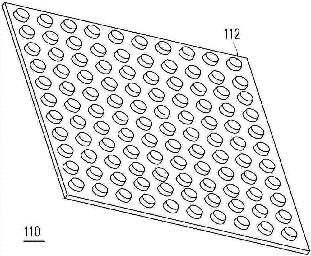
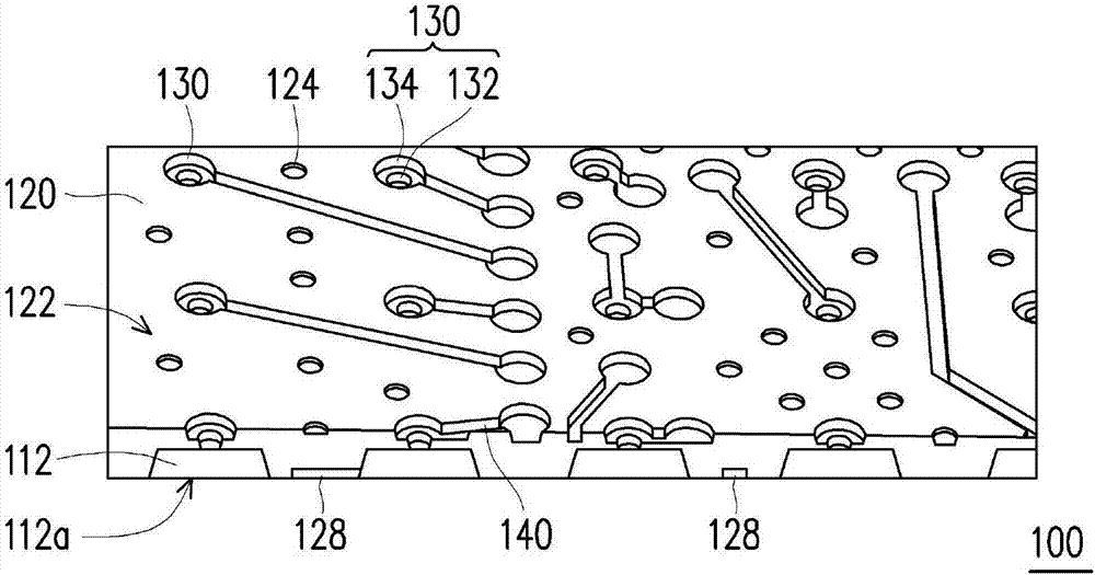
[0060] figure 1 is a schematic diagram of a lead frame according to an embodiment of the present invention. figure 2 is a schematic diagram of a packaging structure according to an embodiment of the present invention. image 3 is a partial cross-sectional schematic diagram of a packaging structure according to an embodiment of the present invention. Please also refer to Figure 1 to Figure 3 , the package structure 100 of this embodiment includes a lead frame 110 , an optional electroplating epoxy resin 120 , a plurality of first via holes 130 and a first patterned circuit layer 140 . First, provide the figure 1 The lead frame 110 is shown, and the lead frame 110 includes a metal pillar array, which includes a plurality of metal pillars 112 arranged in an array.

[0061] Such as figure 1 The illustrated lead frame 110 can be formed in the following steps. First, a metal substrate is provided. Next, a patterned photoresist layer is formed on the upper surface of the met...


PUM


Abstract

A package structure includes a lead frame, a selective-electroplating epoxy compound, conductive vias and a patterned circuit layer. The lead frame includes a metal stud array having metal studs. The selective-electroplating epoxy compound covers the metal stud array. The selective-electroplating epoxy compound includes non-conductive metal complex. The conductive vias are directly embedded in the selective electroplating epoxy compound to be respectively connected to the metal studs and extended to a top surface of the selective-electroplating epoxy compound. Each of the conductive vias includes a lower segment connected to the corresponding metal stud and an upper segment connected to the lower segment and extended to the top surface, and a smallest diameter of the upper segment is greater than a largest diameter of the lower segment. The patterned circuit layer is directly disposed on the top surface and electrically connected to the conductive vias. The technical scheme can simplify the processing technology, narrow the overall thickness and improve the circuit design elasticity.

Description

technical field [0001] The present invention relates to a package structure, and in particular to a package structure which can be directly electroplated on the optional electroplating epoxy resin to form a patterned circuit layer. Background technique [0002] In today's information society, human beings are increasingly dependent on electronic products. In order to meet the requirements of high speed, high performance, light weight and short size of today's electronic products, flexible circuit boards with flexible characteristics have been gradually used in various electronic devices, such as: mobile phones (Mobile Phone), notebook computers (Notebook PC) ), digital camera (digital camera), tablet computer (tablet PC), printer (printer) and CD player (disk player), etc. [0003] Generally speaking, the production of circuit boards is mainly to carry out pretreatment, sputtering (sputter), copper pressing or electroplating on one side or two opposite surfaces of the insul...

Claims


Application Information

Patent Timeline
Patent Type & Authority Applications(China)
IPC IPC(8): H01L23/498H01L23/492
CPCH01L23/49517H01L23/498H01L23/49811H01L2224/48091H01L2924/181H01L2924/00014H01L2924/00012
Inventor 刘文俊
Owner IBIS INNOTECH
Learn More