


Quick Research
Generate reliable direction feasibility study reports for your R&D in just a few steps.

Technical Q&A
Discover and master advanced knowledge NOW. Basics, ideas, possibilities, all at once.

Find Solutions
As an expert in R&D theories, this can generate solutions to your technical problems instantly.

Evaluate Feasibility
Analyze your overall solution with one click, know your potential R&D risks in advance.

Monitor Landscape
Get weekly tech updates, stay abreast of the latest tech innovations and key insights.
Semiconductor chip aging test device and method
A chip aging test and aging test technology, which is applied in the direction of measurement device, electronic circuit test, measurement power, etc., can solve the problems of aging test accuracy and frequency distortion affecting semiconductor chips, achieve fast selection, and overcome impedance mismatch. , to ensure the effect of accuracy
- Summary
- Abstract
- Description
- Claims
- Application Information
AI Technical Summary
Problems solved by technology
Method used
Image

Examples
Embodiment 1
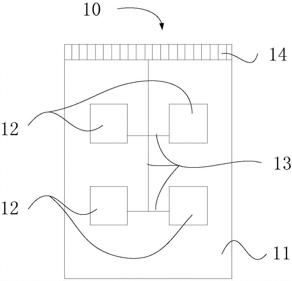
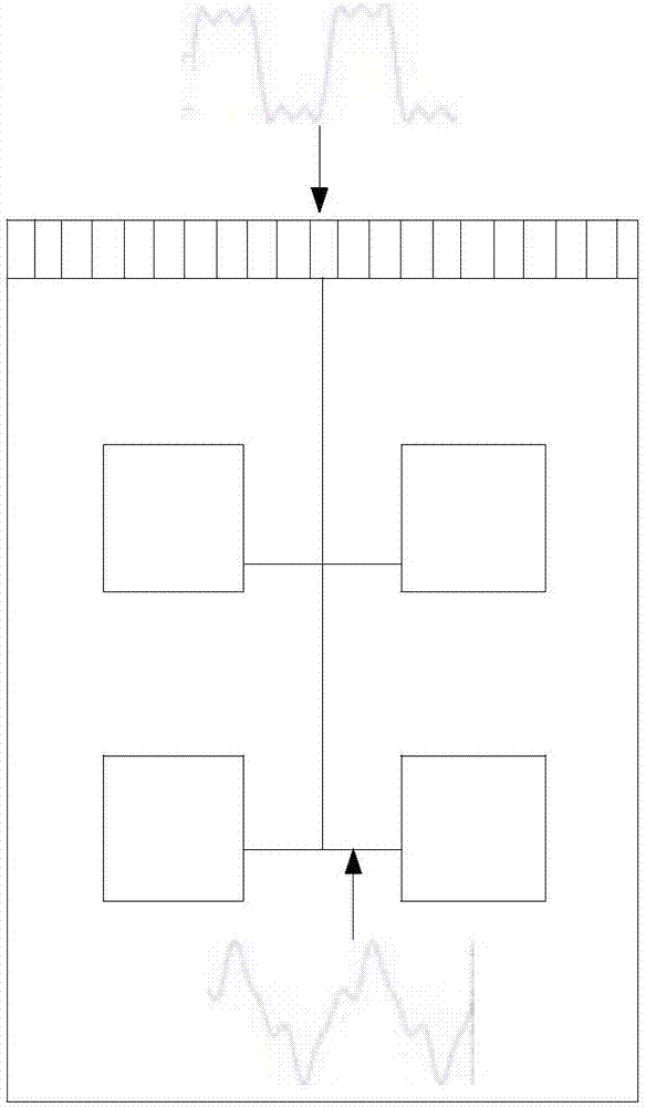
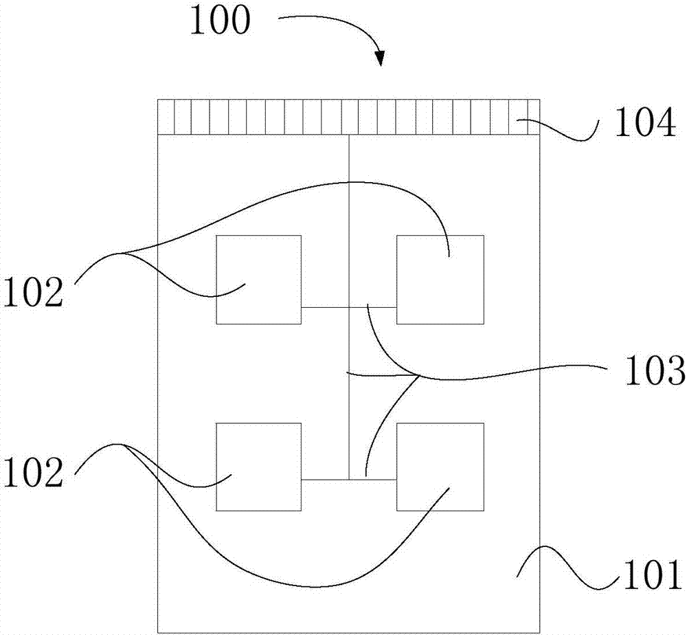
[0035] image 3 It is a structural schematic diagram of a test burn-in board of a burn-in test device for a semiconductor chip of the present invention; Figure 4 It is a schematic structural view of an embodiment of the burn-in testing device for semiconductor chips of the present invention; as Figure 3-4 As shown, in the semiconductor chip burn-in testing device provided in the first embodiment, the semiconductor chip is a flash memory. Of course, it may also be other types of semiconductor memory chips or other types of semiconductor chips, not limited to flash memory or memory. In this embodiment, the multiplexer MUX with two signal input terminals IN is selected to be used, that is, the multiplexer MUX that chooses one of the two. It is only used to perform burn-in tests on any two of the three modes of the write mode, read mode and erase mode of the semiconductor flash memory chip burn-in test device; wherein, the two signal input terminals IN of the multiplexer MUX ...
Embodiment 2
[0037] image 3 It is a structural schematic diagram of a test burn-in board of a burn-in test device for a semiconductor chip of the present invention; Figure 5 It is a schematic structural view of another embodiment of the burn-in testing device for semiconductor chips of the present invention; as image 3 , Figure 5 As shown, in the semiconductor chip burn-in testing device provided in the second embodiment, the semiconductor chip is a flash memory. Choose to use a multiplexer MUX with four signal input terminals IN, that is, a multiplexer MUX that selects one from four. The three signal input terminals IN of the multiplexer MUX described therein are connected with high-frequency crystal oscillators X of different frequencies, which are used for semiconductor flash memory in three modes of writing mode, reading mode and erasing mode The chip carries out the aging test of all modes. The multiplexer MUX in this embodiment refers to a multiplexer MUX with multiple signal...
Embodiment 3
[0044] The present embodiment three provides a semiconductor chip aging test method based on the above-mentioned embodiment one or embodiment two, adopts the semiconductor chip aging test device as above-mentioned embodiment one or embodiment two, and its scheme is as follows: through multiplexer The control circuit 200 composed of MUX and a plurality of high-frequency crystal oscillators X applies a frequency signal to the chip socket 102 of the test burn-in board 100, when the signal input terminal IN of the multiplexer MUX is connected with a high-frequency crystal oscillator X, and when the signal control terminal IN is strobe-connected with the signal input terminal IN of the high-frequency crystal oscillator X, the signal output terminal OUT of the multiplexer MUX outputs a certain high-frequency frequency test signal and load the test signal to the chip socket 102 of the test burn-in board 100, so as to perform burn-in test on the semiconductor chip to be burn-in tested ...
PUM
 Abstract
Description
Claims
Application Information
 - R&D Engineer
- R&D Manager
- IP Professional
- Industry Leading Data Capabilities
- Powerful AI technology
- Patent DNA Extraction
Browse by: Latest US Patents, China's latest patents, Technical Efficacy Thesaurus, Application Domain, Technology Topic, Popular Technical Reports.
© 2024 PatSnap. All rights reserved.Legal|Privacy policy|Modern Slavery Act Transparency Statement|Sitemap|About US| Contact US: help@patsnap.com