


Quick Research
Generate reliable direction feasibility study reports for your R&D in just a few steps.

Technical Q&A
Discover and master advanced knowledge NOW. Basics, ideas, possibilities, all at once.

Find Solutions
As an expert in R&D theories, this can generate solutions to your technical problems instantly.

Evaluate Feasibility
Analyze your overall solution with one click, know your potential R&D risks in advance.

Monitor Landscape
Get weekly tech updates, stay abreast of the latest tech innovations and key insights.
MEMS chip
A chip and sensitive film technology, applied in the field of MEMS chips, can solve problems such as stress reduction and inability to fully release, and achieve the effect of improving service life and preventing distortion
- Summary
- Abstract
- Description
- Claims
- Application Information
AI Technical Summary
Problems solved by technology
Method used
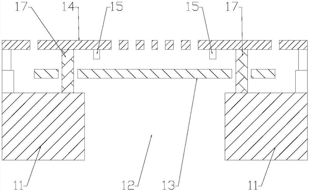
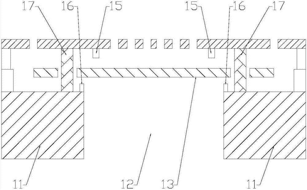
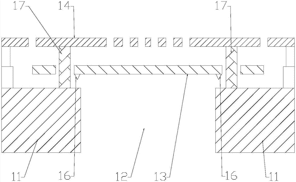
Image

Examples
Embodiment Construction
[0028] Various exemplary embodiments of the present invention will now be described in detail with reference to the accompanying drawings. It should be noted that the relative arrangements of components and steps, numerical expressions and numerical values set forth in these embodiments do not limit the scope of the present invention unless specifically stated otherwise.
[0029] The following description of at least one exemplary embodiment is merely illustrative in nature and in no way taken as limiting the invention, its application or uses.
[0030] Techniques and devices known to those of ordinary skill in the relevant art may not be discussed in detail, but where appropriate, such techniques and devices should be considered part of the description.
[0031] In all examples shown and discussed herein, any specific values should be construed as illustrative only, and not as limiting. Therefore, other instances of the exemplary embodiment may have different values.
...
PUM
 Abstract
Description
Claims
Application Information
 - R&D Engineer
- R&D Manager
- IP Professional
- Industry Leading Data Capabilities
- Powerful AI technology
- Patent DNA Extraction
Browse by: Latest US Patents, China's latest patents, Technical Efficacy Thesaurus, Application Domain, Technology Topic, Popular Technical Reports.
© 2024 PatSnap. All rights reserved.Legal|Privacy policy|Modern Slavery Act Transparency Statement|Sitemap|About US| Contact US: help@patsnap.com