Method for producing image display device, curable resin composition used in the method, touch panel, and image display device
A technology of image display device and curable resin, which can be applied to non-polymer organic compound adhesive, identification device, bonding method, etc., and can solve the problems of visibility, liquid crystal cell gap change, and ripples.
- Summary
- Abstract
- Description
- Claims
- Application Information
AI Technical Summary
Problems solved by technology
Method used
Image


Examples
no. 1 approach
[0057] figure 1 It is a process diagram which shows 1st Embodiment of the manufacturing process of the image display apparatus (it is also called "optical member") of this invention.
[0058] This method is a method of obtaining an optical member by bonding the liquid crystal display unit 1 and the protective plate 2 together.
[0059] The liquid crystal display unit 1 is a liquid crystal display unit including a polarizing plate, a driving circuit, a signal input cable, and a backlight unit on a member in which a liquid crystal material is sealed between a pair of substrates on which electrodes are formed.
[0060] figure 2 It is a cross-sectional view showing a main part of an example of the liquid crystal display unit 1 . like figure 2 As shown, the liquid crystal display unit 1 has a configuration in which a polarizing plate 22 is arranged on a liquid crystal display cell 21 , and a sealing body 23 is arranged on the liquid crystal display cell 21 so as to surround th...
no. 2 approach
[0150] Figure 4 It is a process chart which shows 2nd Embodiment of the manufacturing process of the optical member of this invention.
[0151] This method is a method of obtaining an optical member (image display device) by bonding the liquid crystal display unit 1 and the protective plate 2 together. It should be noted that, for the parts other than the changed parts compared with the first embodiment, the matters described in each of the above-mentioned first embodiment can be reflected and incorporated, and a part of descriptions that duplicate the descriptions are omitted.
[0152] [Process A]
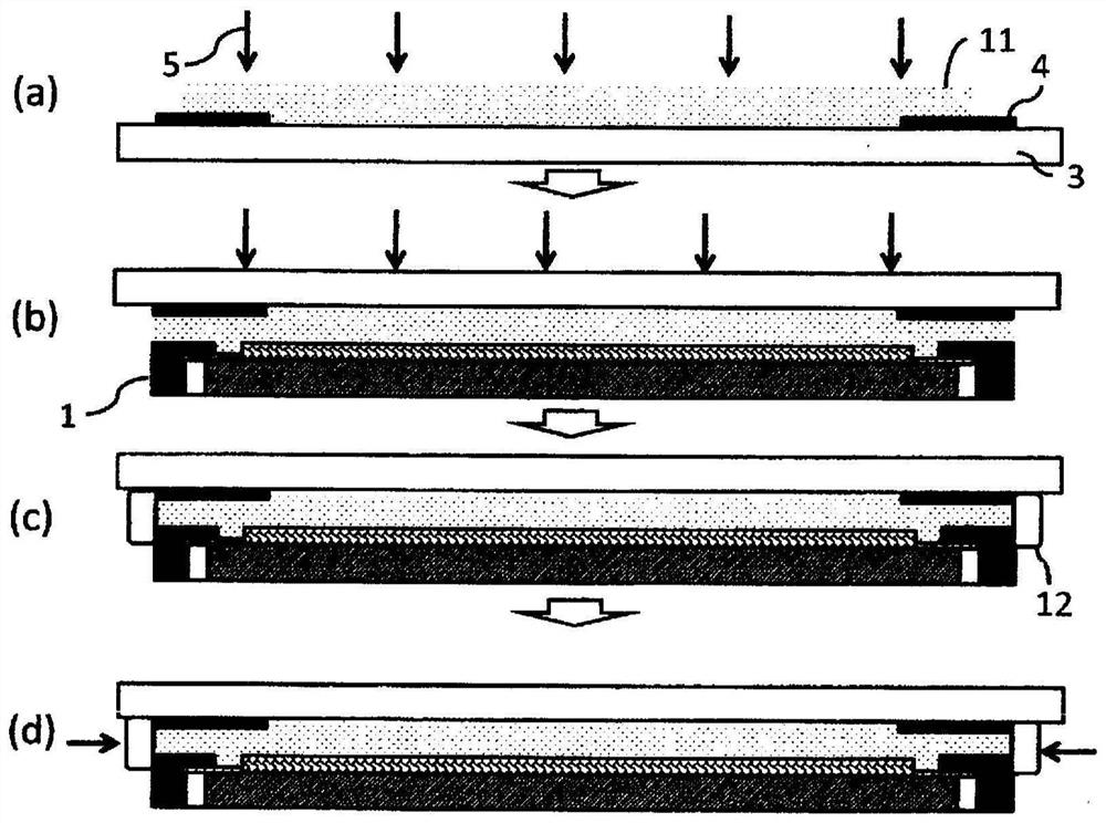
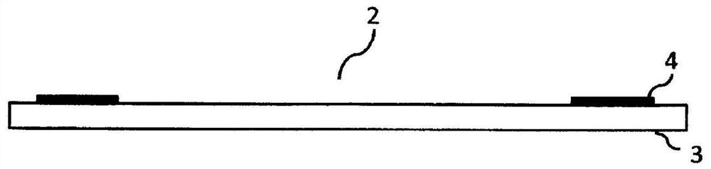
[0153] First, as Figure 4 As shown in (a), a first curable resin composition 11 containing a (meth)acrylate (A) and a photopolymerization initiator (B), which will be described later, is applied to the protective plate 2 having the light-shielding portion 4 formed thereon. on the surface of the surface of the light shielding portion 4 . As a coating method, a slit coater, a ...
no. 3 approach
[0178] Figure 5 It is a process chart which shows 3rd Embodiment of the manufacturing process of the optical member of this invention.
[0179] This method is a method of obtaining an optical member (image display device) by bonding the liquid crystal display unit 1 and the protective plate 2 together. It should be noted that, for the parts other than the changed parts compared with the first embodiment, the matters described in each of the above-mentioned first embodiment can be reflected and incorporated, and a part of descriptions that duplicate the descriptions are omitted.
[0180] [Process A]
[0181] First, as Figure 5 As shown in (a), a first curable resin composition 11 containing a (meth)acrylate (A) and a photopolymerization initiator (B), which will be described later, is applied to the protective plate 2 having the light-shielding portion 4 formed thereon. on the surface of the surface of the light shielding portion 4 . As a coating method, a slit coater, a ...
PUM
| Property | Measurement | Unit |
|---|---|---|
| thickness | aaaaa | aaaaa |
| thickness | aaaaa | aaaaa |
| thickness | aaaaa | aaaaa |
Abstract
Description
Claims
Application Information
 - R&D
- Intellectual Property
- Life Sciences
- Materials
- Tech Scout
- Unparalleled Data Quality
- Higher Quality Content
- 60% Fewer Hallucinations
Browse by: Latest US Patents, China's latest patents, Technical Efficacy Thesaurus, Application Domain, Technology Topic, Popular Technical Reports.
© 2025 PatSnap. All rights reserved.Legal|Privacy policy|Modern Slavery Act Transparency Statement|Sitemap|About US| Contact US: help@patsnap.com