


Quick Research
Generate reliable direction feasibility study reports for your R&D in just a few steps.

Technical Q&A
Discover and master advanced knowledge NOW. Basics, ideas, possibilities, all at once.

Find Solutions
As an expert in R&D theories, this can generate solutions to your technical problems instantly.

Evaluate Feasibility
Analyze your overall solution with one click, know your potential R&D risks in advance.

Monitor Landscape
Get weekly tech updates, stay abreast of the latest tech innovations and key insights.
Method for thermal annealing and semiconductor device formed by method
A technology of semiconductors and power semiconductors, applied in the fields of semiconductor devices, semiconductor/solid-state device manufacturing, chemical instruments and methods, etc., which can solve problems such as processing faults and limiting processing scope
- Summary
- Abstract
- Description
- Claims
- Application Information
AI Technical Summary
Problems solved by technology
Method used
Image


Examples
Embodiment approach
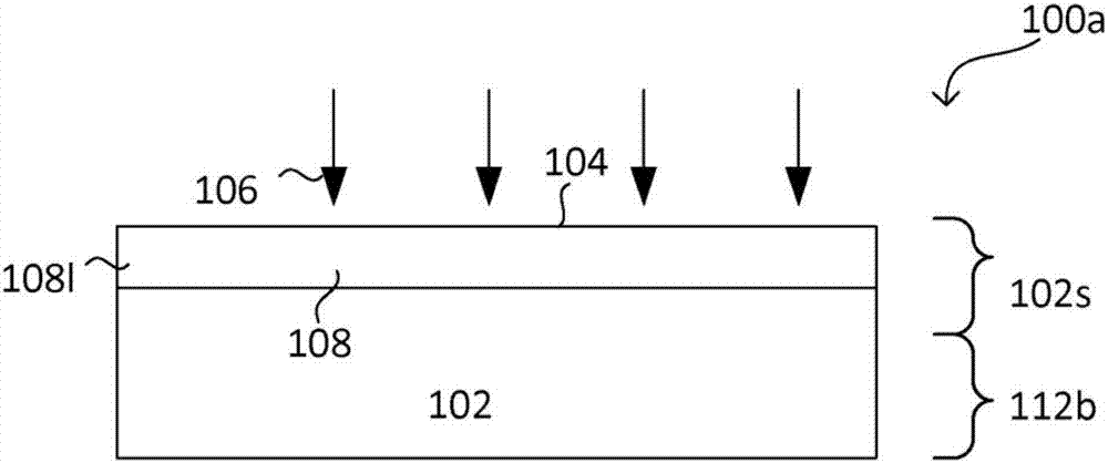
[0207] According to various embodiments, a method may include: disposing a dopant in a semiconductor region (for example, through the surface of the semiconductor region); on at least a portion of the semiconductor region (for example, on one or more portions of the semiconductor region) On or on the entire semiconductor region) forming at least one allotrope including carbon or a radiation absorbing layer formed of at least one allotrope of carbon; and irradiating the radiation absorbing layer at least partially by using electromagnetic radiation to at least partially The semiconductor region is heated to at least partially activate the dopant.
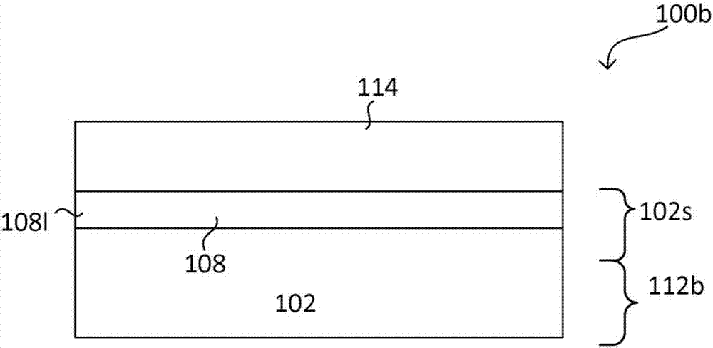
[0208] According to various embodiments of the present invention, a method may include: arranging a dopant in the semiconductor region on a first side of the semiconductor region; forming on at least a part of the semiconductor region on the first side of the semiconductor region A radiation absorbing layer; at least partially activatin...
PUM
 Abstract
Description
Claims
Application Information
 - R&D Engineer
- R&D Manager
- IP Professional
- Industry Leading Data Capabilities
- Powerful AI technology
- Patent DNA Extraction
Browse by: Latest US Patents, China's latest patents, Technical Efficacy Thesaurus, Application Domain, Technology Topic, Popular Technical Reports.
© 2024 PatSnap. All rights reserved.Legal|Privacy policy|Modern Slavery Act Transparency Statement|Sitemap|About US| Contact US: help@patsnap.com