Graphene electrode, patterning preparation method of graphene electrode and array substrate
A graphene electrode and patterning technology, applied in circuits, electrical components, electrical solid devices, etc., can solve the problems of limiting the application of electronic devices, complicated preparation process, and high production cost, achieving low patterning difficulty, simple preparation process, The effect of low production cost
- Summary
- Abstract
- Description
- Claims
- Application Information
AI Technical Summary
Problems solved by technology
Method used
Image

Examples
Embodiment 1
[0048] In order to solve the above-mentioned technical problems existing in the prior art, an embodiment of the present invention provides a patterned preparation method of a graphene electrode.
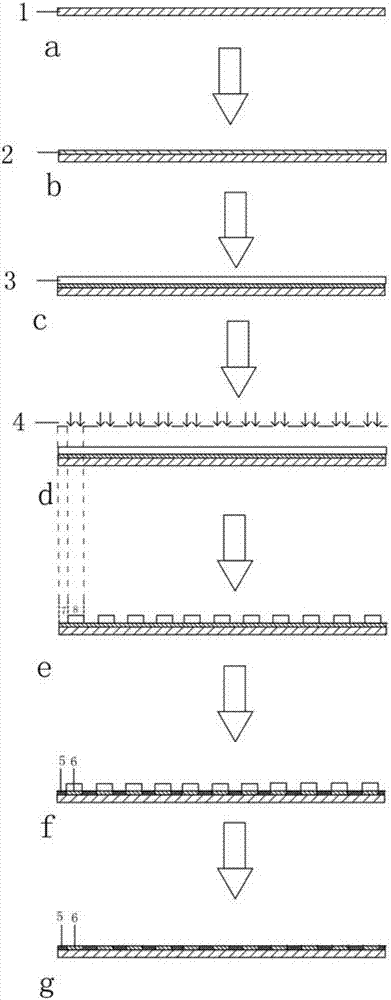
[0049] figure 1 A schematic diagram of the steps of the patterned preparation method of the graphene electrode according to the embodiment of the present invention is shown. refer to figure 1 The patterned preparation method of the graphene electrode in this embodiment includes the following process steps.
[0050] First, a graphene oxide layer 2 and a photoresist layer 3 are sequentially formed on a substrate 1 . Such as figure 1Process a, process b and process c are shown in the process. Specifically, a uniform layer of graphene oxide is first formed on the substrate 1 on which the graphene electrode needs to be formed. Preferably, the method of forming graphene oxide is a solution suspension method, a spin coating method or a slit coating method. After the graphene oxide laye...
Embodiment 2
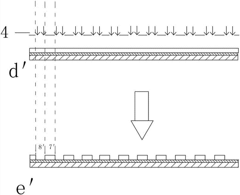
[0060] corresponding, figure 2 A schematic diagram of the process flow of exposing and developing the photoresist layer in the patterned preparation method of the graphene electrode according to another embodiment of the present invention is shown. refer to figure 2 , this embodiment differs from Embodiment 1 in that:
[0061] In the process of forming the graphene oxide layer and the photoresist layer, a positive photoresist is used for the photoresist layer 3 formed on the graphene oxide layer by using a slit coating method (Slit method). The non-exposed areas of the positive photoresist can show the image.
[0062] During the exposure process, such as figure 2 As shown in the d' process, the mask tool is arranged in parallel above the positive photoresist layer, and then the ultraviolet light is irradiated on the photoresist layer 3 through the mask tool vertically, so that the photoresist layer 3 is Fully exposed. Preferably, the mask tool is a mask plate 4 with a ...
Embodiment 3
[0069] Correspondingly, the embodiment of the present invention also provides a graphene electrode prepared by using the graphene electrode patterning method of the first embodiment or the second embodiment.
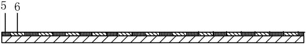
[0070] image 3 A schematic cross-sectional view of a patterned graphene electrode manufactured by using a patterned graphene electrode preparation method according to an embodiment of the present invention is shown.
[0071] refer to image 3 In this embodiment, the graphene electrode is located in the graphene electrode layer. The patterned graphene electrode prepared by the above method has the following advantages: low cost, wide application range, easier processing and utilization, and better conductivity.
[0072] Here, the upper surface of the layer where the graphene electrodes are located is parallel to the upper surface of the substrate 1 . Apply the patterned graphene electrode of the present embodiment, because the upper surface of graphene electrode layer...
PUM
 Abstract
Description
Claims
Application Information
 - Generate Ideas
- Intellectual Property
- Life Sciences
- Materials
- Tech Scout
- Unparalleled Data Quality
- Higher Quality Content
- 60% Fewer Hallucinations
Browse by: Latest US Patents, China's latest patents, Technical Efficacy Thesaurus, Application Domain, Technology Topic, Popular Technical Reports.
© 2025 PatSnap. All rights reserved.Legal|Privacy policy|Modern Slavery Act Transparency Statement|Sitemap|About US| Contact US: help@patsnap.com