
A method for preparing Si fixed-point substitution amorphous nanowire array

A nanowire array, amorphous technology, used in the field of template-free preparation of Si fixed-point substitution of amorphous nanowire arrays, can solve the problems of unfavorable carrier transfer to the surface, reduced photocatalytic efficiency, harsh preparation conditions, etc. Novel and uniform appearance, high light utilization efficiency and simple preparation process

Inactive Publication Date: 2019-01-25
TONGJI UNIV
View PDF1 Cites 0 Cited by
  • Summary
  • Abstract
  • Description
  • Claims
  • Application Information

AI Technical Summary

Problems solved by technology

So far, people have studied and prepared crystalline Zn with different morphologies. 2 GeO 4 materials, but the preparation of ultrafine, high aspect ratio Zn 2 GeO 4 Nanowire arrays often have problems such as harsh preparation conditions (usually need to add surfactants or structure-directing agents, etc.), complex processes and expensive costs.
The morphology prepared by the hydrothermal method with mild preparation conditions is mostly nano-short rods with small aspect ratios. Compared with nanowires, it is not conducive to the transfer of carriers from the interior to the surface, which greatly reduces the photocatalytic (photoelectric conversion) efficiency
Therefore, for amorphous Zn 2 GeO 4 or based on Zn 2 GeO 4 The preparation of nanowire arrays still faces great challenges

Method used


Image

  • A method for preparing Si fixed-point substitution amorphous nanowire array
  • A method for preparing Si fixed-point substitution amorphous nanowire array
  • A method for preparing Si fixed-point substitution amorphous nanowire array

Examples


Embodiment 1

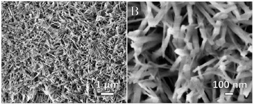
[0029] 0.55g of zinc acetate and 0.13g of germanium oxide were weighed and added to a mixed solvent of 10ml of water and 20ml of ethylenediamine. Stir magnetically at room temperature for one hour at a stirring rate of 600 r / min. Transfer the mixed solution to a 50ml reaction kettle, and put into a single crystal Si chip (1.5*3cm 2 ), 150 degree hydrothermal reaction for 10h. After cooling to room temperature, the product was washed alternately with ethanol and deionized water. The samples prepared as figure 1 As shown in A, it is a nanowire array structure with uniform shape and stable structure. It can be observed from 1B that the diameter of the nanowire array is about 40-60 nm.

Embodiment 2

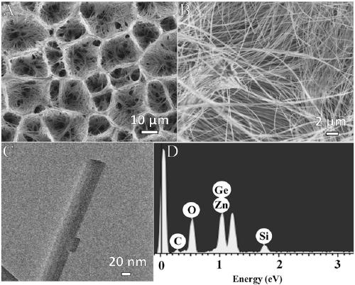
[0031] 0.55g of zinc acetate and 0.13g of germanium oxide were weighed and added to a mixed solvent of 10ml of water and 20ml of ethylenediamine. Stir magnetically at room temperature for one hour at a stirring rate of 800 r / min. Transfer the mixed solution to a 50ml reaction kettle, and put into a single crystal Si chip (1.5*3cm 2 ), 180 degree hydrothermal reaction for 15h. After cooling to room temperature, the product was washed alternately with ethanol and deionized water. The samples prepared as figure 2 As shown in A, it is a honeycomb nanowire array structure. The product has a unique shape and is evenly distributed.

Embodiment 3

[0033] 0.55g of zinc acetate and 0.13g of germanium oxide were weighed and added to a mixed solvent of 10ml of water and 20ml of ethylenediamine. Stir magnetically at room temperature for one hour at a stirring rate of 1000 r / min. Transfer the mixed solution to a 50ml reaction kettle, and put into a single crystal Si chip (1.5*3cm 2 ), 180 degree hydrothermal reaction for 20h. After cooling to room temperature, the product was washed alternately with ethanol and deionized water. The samples prepared as figure 2 As shown in B, it is an ultra-long nanowire array with a length of about tens of microns.


PUM

PropertyMeasurementUnit
diameteraaaaaaaaaa
diameteraaaaaaaaaa

Abstract

The invention relates to a method for preparing a fixed-point replaced amorphous nanowire array with Si. The method includes the steps that (1) zinc acetate and germanium oxide are added into a mixed solvent of water and ethylenediamine; (2) the mixture obtained from the step (1) is stirred with magnetic force to obtain a homogeneous solution; (3) pretreatment is conducted on a monocrystal Si piece, and then washing and drying are conducted; (4) the pretreated monocrystal Si piece is added in the homogeneous solution obtained from the step (2), and then a hydrothermal reaction is conducted; (5) the reaction product is cooled, washed and dried, and a final product is obtained on the Si piece. Compared with the prior art, the preparation method is novel, repeatability is good, the product property is stable, the product has a larger specific surface area and higher surface activity and light utilization efficiency, and the product can be widely applicable to many energy storage fields of photoelectric devices, solar cells, lithium-ion batteries, supercapacitors and the like.

Description

technical field [0001] The invention relates to a preparation method used as a photoelectric energy storage device material, in particular to a method for preparing Si fixed-point substitution amorphous nanowire arrays without a template. Background technique [0002] Semiconductor nanomaterials have attracted much attention due to their special optoelectronic properties and great potential in the fields of energy and environment. At present, most of the semiconductor nanomaterials involved in the research are crystalline. Relatively speaking, amorphous semiconductor materials theoretically have many advantages in optoelectronic devices, such as higher specific surface area, higher surface activity and higher light utilization efficiency. However, due to the difficulty in synthesis of amorphous semiconductor nanomaterials, the research is very limited, which greatly limits the development of amorphous semiconductor materials. Secondly, one-dimensional semiconductor nanostr...

Claims


Application Information

Patent Timeline
Patent Type & Authority Patents(China)
IPC IPC(8): C01B33/00C01B3/04
CPCC01B3/042C01B33/00C01P2002/72C01P2004/03C01P2004/04C01P2004/16C01P2004/52C01P2004/64C01P2006/40Y02E60/36
Inventor 杨金虎贺婷张棪刘光磊
Owner TONGJI UNIV
Learn More