Laser direct writing data processing system and processing method

A data processing system and laser direct writing technology, applied in optics, opto-mechanical equipment, microlithography exposure equipment, etc., can solve the problems of large data transmission, long data link, and many fault points, and shorten the data link. The effect of reducing the number of roads, reducing nodes, and reducing workload

Inactive Publication Date: 2017-08-18
ADVANCED DIGITAL SCREEN SYST INC
View PDF6 Cites 6 Cited by
  • Summary
  • Abstract
  • Description
  • Claims
  • Application Information

AI Technical Summary

Problems solved by technology

[0005] In the existing LDI system, slaves and optical fiber transmission boards are often installed between the host and DPB. The data transmission volume between components of this system structure is extremely large, and the data link is long, with many fault points and high cost.

Method used


Image

  • Laser direct writing data processing system and processing method
  • Laser direct writing data processing system and processing method
  • Laser direct writing data processing system and processing method

Examples


Embodiment 1

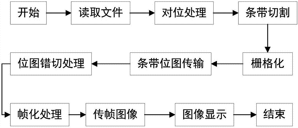
[0055] This embodiment provides a laser direct writing data processing system according to the technical solution of the present invention, as shown in the attached Figure 4 As shown, the system includes a host, a data processing module and a DMD.

[0056] Among them, the data processing module is composed of data receiving unit, FPGA V6, DDR and DLP chipset (see attached Figure 5 )——FPGA V6 is the data processing unit, the model is XC6VLX240T, and DDR is the storage unit. The DLP chipset includes two DLP chips, a FLASH chip and an FPGA V5 chip (see attached Figure 6 )——The FLASH chip is a program storage chip, and the FPGA V5 chip is an image transmission chip.

[0057] The host generally can be a PC, various servers or various industrial computers. By carrying a software system, the host computer can perform corresponding data processing.

[0058] DMD is a commonly used SLM. Under the action of the light source, the DMD projects the received frame image onto the subs...

Embodiment 2

[0078] This embodiment provides another laser direct writing data processing system according to the technical solution of the present invention. Compared with Embodiment 1, the system of this embodiment has some changes in the structure of the data processing module, as shown in the attached Figure 9 As shown, the data processing module in this embodiment is composed of a data receiving unit, an ARM+FPGA, a DDR and a DLP chipset.

[0079] Wherein, the ARM+FPGA corresponds to the FPGA V6 in Embodiment 1, and is a data processing unit, and the ARM+FPGA can also be replaced by an SoC chip, and the mainstream SoC chip manufacturers are Altera or Xilinx.

[0080] In Embodiment 1, the host completes the rasterization of graphics, which requires high computing power of the host; the solution in Embodiment 1 does not support the working conditions of multiple DMDs. However, if the rasterization work is performed by the FPGA, the development of the FPGA is more difficult. In this em...


PUM


Abstract

The invention discloses a laser direct writing data processing system. The laser direct writing data processing system comprises a host, a data processing module and a spatial light modulator (SLM), wherein the data processing module comprises a data receiving unit, a data processing unit, a data storage unit and a digital light processing (DLP) chipset, the DLP chipset comprises a DLP chip, a storage chip and an image transmission chip, the host and the data processing module are connected through a data transmission line, and the data processing module and the SLM are connected by a data wire. The invention also discloses a method for data processing by employing the data processing system. The laser direct writing data processing system is high in integration, concise in processing procedure, small in data transmission quantity among modules and low in cost and is convenient to maintain.

Description

technical field [0001] The invention relates to the technical field of laser direct writing, in particular to a laser direct writing data processing system and processing method. Background technique [0002] Laser direct imaging (laser direct imaging, LDI for short), also known as laser direct writing, is a technology developed in recent years for the exposure process of printed circuit boards (PCB). The traditional exposure process is to transfer the image to the PCB by irradiating the film with a mercury lamp, while LDI is a maskless exposure system that converts the vector graphics into a bitmap with the resolution required for production and projects it onto the PCB through the DMD. Compared with the traditional exposure technology, the LDI exposure process does not require film, which effectively reduces the cost, and has a simple process and high image precision, which can adapt to finer graphic exposure and is also conducive to improving the yield rate of PCB product...

Claims


Application Information

Patent Timeline
IPC IPC(8): G03F7/20
CPCG03F7/70383G03F7/70508
Inventor 王运钢陈修涛韩非高明吴景舟
Owner ADVANCED DIGITAL SCREEN SYST INC
Why Eureka
Try Eureka