
Aging compensation system and method for oled devices

A compensation system and compensation method technology, applied in the direction of instruments, static indicators, etc., can solve the problems such as the decrease of the display brightness of the display mura, the inability to improve the problem of the gradual decrease of the display brightness and the afterimage problem, and the decline of the display effect of the OLED display. Improve display afterimage problem, improve brightness drop, improve the effect of uniformity

Active Publication Date: 2019-08-13
SHENZHEN CHINA STAR OPTOELECTRONICS SEMICON DISPLAY TECH CO LTD
View PDF5 Cites 0 Cited by
  • Summary
  • Abstract
  • Description
  • Claims
  • Application Information

AI Technical Summary

Problems solved by technology

With the use of OLED displays, even if the same amount of current flows through OLED devices after aging, the organic materials in them will age, which will reduce the display effect of OLED displays, resulting in a gradual decrease in display mura (spots) and display brightness.
[0009] In the prior art, aging compensation for OLED displays generally only compensates for display mura caused by OLED displays
However, it cannot improve the problem of gradual decrease in display brightness and afterimage problem

Method used


Image

  • Aging compensation system and method for oled devices
  • Aging compensation system and method for oled devices
  • Aging compensation system and method for oled devices

Examples


Embodiment

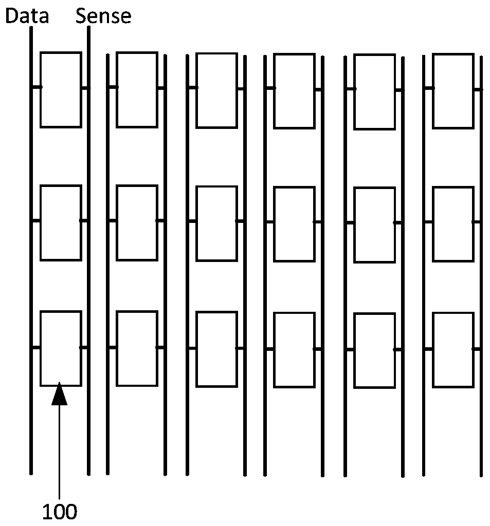
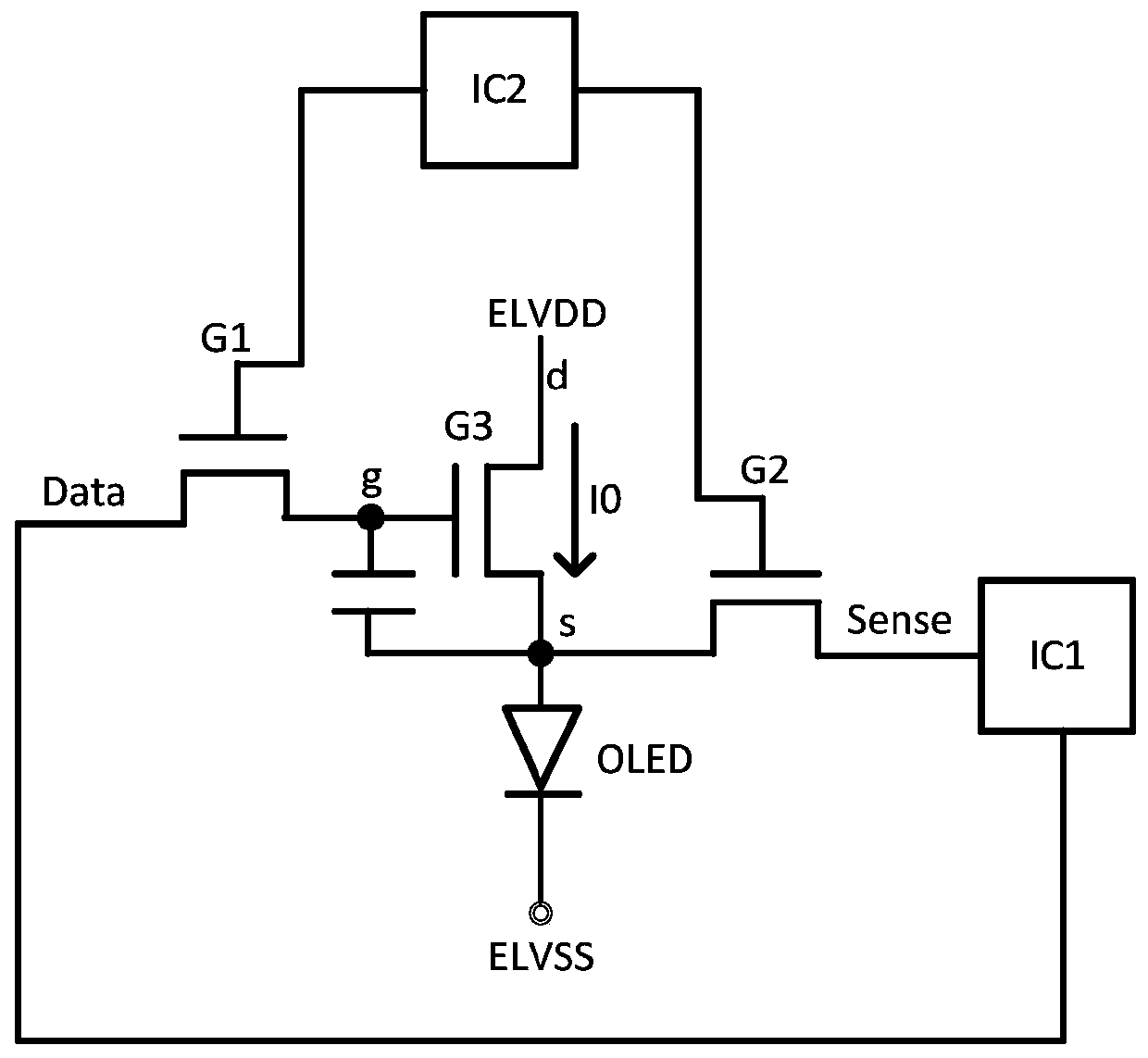
[0066] As a specific embodiment of the present invention, such as Figure 1 to Figure 4 As shown, the embodiment of the present invention discloses an aging compensation system and a sensing and compensation method of an OLED device. The aging compensation system includes a pixel circuit 100, a data line Data, a sensing line Sense, a first power supply ELVDD, a second power supply ELVSS, a source driver chip IC1 and a gate driver chip IC2.

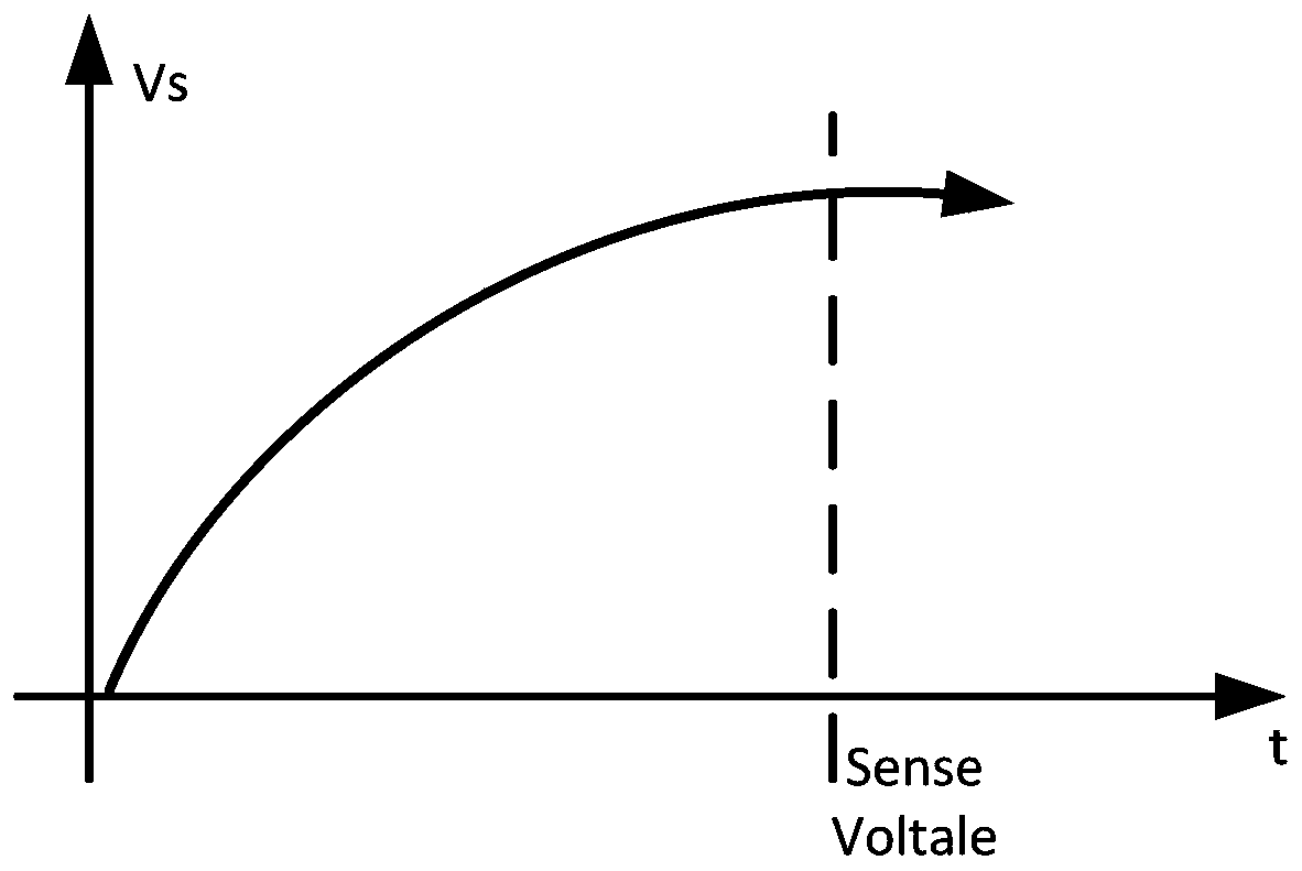
[0067] It should be noted, figure 1 and figure 2 Data in means the data line, Sense means the sensing line, and Figure 4 Among them, Senseline represents the signal sensed by the sense line.

[0068] Wherein, there are multiple pixel circuits, one of which includes an OLED device, such as figure 2 OLED shown. Further, the pixel circuit shown further includes a driving transistor G3, a first transistor G2, a second transistor G1 and a capacitor Cst. Wherein, the driving transistor, the first transistor and the second transistor are...


PUM


Abstract

An ageing compensation system and method for an OLED device, the ageing compensation system for the OLED device comprising a pixel circuit (100), data lines (Data), sensing lines (Sense), a first power source ELVDD, a second power source ELVSS, and a source electrode drive chip IC1, the pixel circuit (100) comprising an OLED device and a drive transistor G3. The number of sensing lines (Sense) and data lines (Data) is the same, one sensing line (Sense) coordinating with one data line (Data), and also being connected to a plurality of pixel circuits (100), the sensing lines (Sense) being connected to an anode of the OLED device by means of a first transistor G2, and being used for sensing the voltage VOLED of the OLED device; the first power source ELVDD is connected to the drive transistor G3 and the second power source ELVSS is connected to the cathode of the OLED device; the electrode drive chip IC1 is connected to the data lines (Data), and is used for transmitting the image voltage; and the source electrode drive chip IC1 is connected to a sensing line (Sense), in order to find the current light emitting efficiency in a look-up table, obtain a compensation voltage after calculation, and perform ageing compensation of the OLED device. The problem of reduced brightness due to ageing of the OED device is improved, the problem of residual image display is improved, and the uniformity of the OLED display screen is improved.

Description

[0001] 【Technical field】 [0002] The invention relates to the field of display technology, in particular to an aging compensation system and method for OLED devices. [0003] 【Background technique】 [0004] Existing displays mainly include liquid crystal displays and OLED displays. [0005] Liquid crystal display has many advantages such as thin body, power saving, small radiation, etc., and has been widely used. Most of the liquid crystal displays currently on the market are backlight liquid crystal displays, which include a liquid crystal panel and a backlight module (Backlight Module). The working principle of the liquid crystal panel is to place liquid crystal molecules between two parallel glass substrates, and apply a driving voltage on the two glass substrates to control the rotation direction of the liquid crystal molecules, so as to transmit the light from the backlight module to produce a picture. [0006] Among them, Thin Film Transistor-Liquid Crystal Display (TF...

Claims


Application Information

Patent Timeline
Patent Type & Authority Patents(China)
IPC IPC(8): G09G3/3208
CPCG09G3/3208G09G2320/0233
Inventor 解红军
Owner SHENZHEN CHINA STAR OPTOELECTRONICS SEMICON DISPLAY TECH CO LTD
Learn More