Metal growth method based on single atomic layer deposition

A single atomic layer and growth method technology, which is applied in the direction of metal material coating process, coating, gaseous chemical plating, etc., can solve problems such as device instability, resistivity increase, work function drift, etc., to improve device reliability properties, the effect of reducing resistivity

Inactive Publication Date: 2017-07-28
INST OF MICROELECTRONICS CHINESE ACAD OF SCI
View PDF3 Cites 3 Cited by
  • Summary
  • Abstract
  • Description
  • Claims
  • Application Information

AI Technical Summary

Problems solved by technology

However, since ALD is not a high-vacuum reaction process, the control of water and oxygen is technically more difficult
When excess oxygen exists in the ALD metal film, it will not only cause an increase in resistivity, but also cause a shift in the work function, which will bring great instability to the device

Method used


Image

  • Metal growth method based on single atomic layer deposition
  • Metal growth method based on single atomic layer deposition
  • Metal growth method based on single atomic layer deposition

Examples


Embodiment Construction

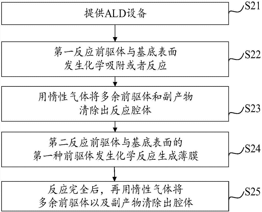
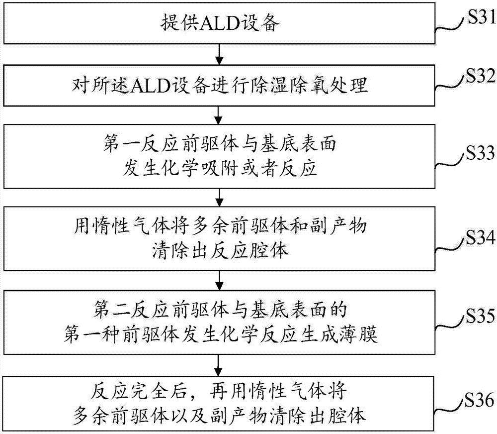
[0033] In order to make the purpose, technical solutions and advantages of the embodiments of the present invention clearer, the technical solutions in the embodiments of the present invention will be clearly and completely described below in conjunction with the drawings in the embodiments of the present invention. Obviously, the described embodiments It is only some embodiments of the present invention, but not all embodiments. Based on the embodiments of the present invention, all other embodiments obtained by persons of ordinary skill in the art without making creative efforts belong to the protection scope of the present invention.

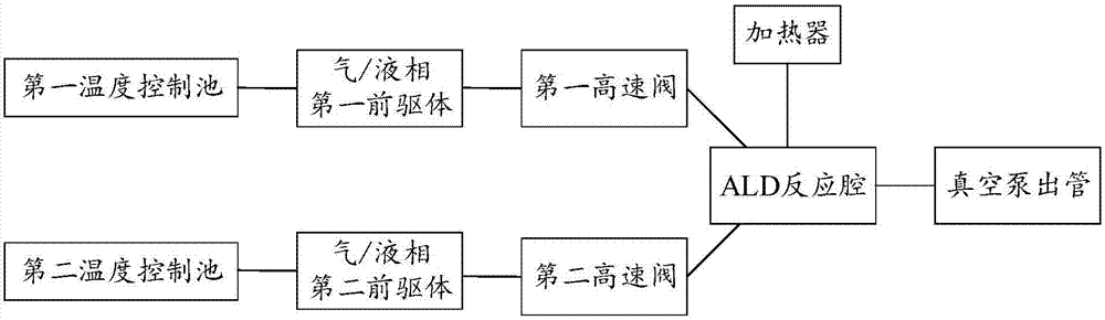
[0034] In the prior art, monoatomic layer deposition (ALD) alternately feeds gas phase precursors into the reaction chamber and deposits them on the substrate for chemical adsorption, and reacts to form a monolayer deposition film. The surface reaction of ALD has chemical adsorption self-limitation (CS) and sequential reaction self-limitation...


PUM


Abstract

The invention provides a metal growth method based on single atomic layer deposition. The method comprises the steps as follows: single atomic layer deposition equipment is provided; dehumidification and oxygen removal treatment is performed on a single atomic layer deposition reaction chamber in the single atomic layer deposition equipment; first precursor reactants are introduced into the reaction chamber and react on the surface of a substrate; the redundant first precursor reactants and reaction by-products are discharged from the reaction chamber; second precursor reactants are introduced into the reaction chamber and react with the first precursor reactants on the substrate; and the redundant second precursor reactants and reaction by-products are discharged from the reaction chamber. With the metal growth method based on single atomic layer deposition, the water oxygen content in the single atomic layer deposition (ALD) equipment can be reduced, and the method is applicable to control on the oxygen content of metal gate materials in integrated circuits and can also be applied in any film forming fields.

Description

technical field [0001] The invention relates to the technical field of microelectronic device manufacturing, in particular to a metal growth method based on monoatomic layer deposition. Background technique [0002] At present, the size of transistors is shrinking rapidly, and the performance is continuously improving. Integrating more devices on a chip with the same area can make the integrated circuit more powerful and reduce the unit function cost. However, when the size of traditional polysilicon gate transistors is reduced to a certain extent, excessive gate resistance and polysilicon depletion effects will hinder the improvement of transistor performance. After a lot of research, the refractory metal gate is considered to be the most promising alternative technology. Using titanium, tantalum and other alloys as the gate electrode can obtain a very low gate sheet resistance and fundamentally eliminate the depletion effect of the polysilicon gate. Obtain a lower equival...

Claims


Application Information

Patent Timeline
IPC IPC(8): C23C16/455C23C16/06
CPCC23C16/45525C23C16/06C23C16/4408
Inventor 项金娟王晓磊杨红王文武赵超
Owner INST OF MICROELECTRONICS CHINESE ACAD OF SCI
Why Eureka
Try Eureka