Touch control substrate and display panel

A technology for display panels and substrates, applied in the fields of instruments, electrical digital data processing, electrical components, etc., can solve the problem of single function of the touch panel, and achieve the effect of accurate fingerprint information

Active Publication Date: 2017-07-21
BOE TECH GRP CO LTD
View PDF6 Cites 29 Cited by
  • Summary
  • Abstract
  • Description
  • Claims
  • Application Information

AI Technical Summary

Problems solved by technology

[0004] The technical problems to be solved by the present invention include, aiming at the single-function problem of the existing touch panel, providing a touch substrate and a display panel capable of fingerprint recognition

Method used


Image

  • Touch control substrate and display panel
  • Touch control substrate and display panel
  • Touch control substrate and display panel

Examples


Embodiment 1

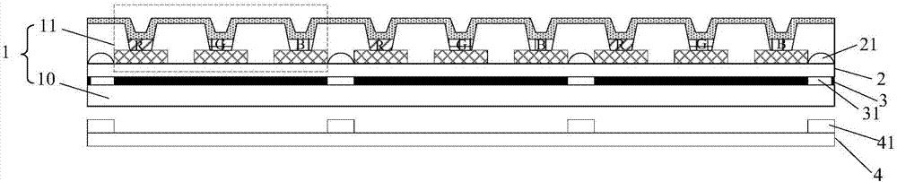
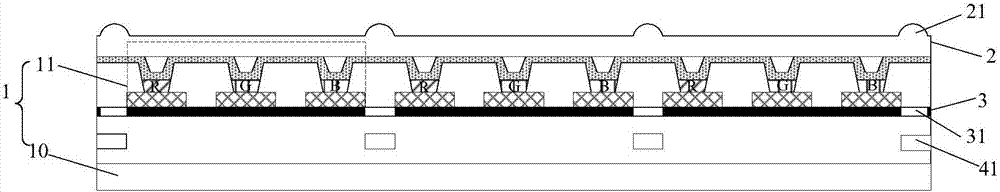
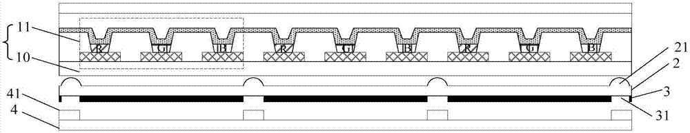
[0040] to combine Figures 1 to 3 As shown, the present embodiment provides a touch substrate, which is arranged opposite to the glass cover 5 to form a touch panel with a fingerprint identification function. The touch substrate specifically includes: a lens array 2, a pixel array 1, a photosensitive device array 4, and a light shielding layer 3; wherein, the lens array 2 includes a plurality of lens units 21; the pixel array 1 includes a plurality of pixel units 11, and One lens unit 21 is correspondingly arranged between two adjacent pixel units 11; the photosensitive device array 4 is located below the pixel array 1, and the photosensitive device array 4 includes a plurality of photosensitive devices 41, and each A photosensitive device 41 is provided corresponding to a lens unit 21; the light-shielding layer 3 is located on the side of the lens array 2 close to the photosensitive device array 4, and a plurality of via holes 31 are arranged in the light-shielding layer 3, a...

Embodiment 2

[0048] Such as Figure 4 As shown, this embodiment provides a display device, which includes the touch substrate in the embodiment, and a cover plate 5 disposed opposite to the touch substrate. Of course, an encapsulation layer 6, a polarizer 7 and an optical adhesive layer 8 are sequentially arranged above the layer where the cathode of each sub-pixel (OLED device) of the touch control substrate is located; wherein the encapsulation layer 6 is used to encapsulate the OLED device to To prevent external water vapor, particles, etc. from polluting the OLED device; the polarizer 7 is used to prevent glare; the optical adhesive (OCA) layer 8 is used to bond the touch substrate and the cover plate 5 .

[0049] Such as Figure 5 As shown, for the thickness of the cover plate 5 in this embodiment is H, the refractive index is n 1 , the thickness of the lens array 2 of the touch substrate is L, and the refractive index is n 2 The distance between the lens array 2 and the cover plat...


PUM


Abstract

The invention provides a touch control substrate and a display panel, and belongs to the technical field of displaying. The touch control substrate comprises a lens array, a pixel array, a light perception device array and a light shielding layer. The lens array comprises multiple lens units. The pixel array comprises multiple pixel units. One lens unit is correspondingly arranged between two adjacent pixel units. The light perception device array is arranged under the pixel array and comprises multiple light perception devices. Each light perception device is arranged corresponding to one lens unit. The light shielding layer is arranged on one side, near the light perception device array, of the lens array. Multiple via holes are arranged in the light shielding layer. Each via hole is arranged corresponding to one lens unit.

Description

technical field [0001] The invention belongs to the field of display technology, and in particular relates to a touch substrate and a display panel. Background technique [0002] Fingerprints are innate, unique and invariable characteristics of the human body that can be distinguished from others. It is made up of a series of ridges and valleys on the surface of the skin on the fingertips. The compositional details of these ridges and valleys usually include details such as ridge forks, ridge ends, arches, tent-like arches, left-handed, right-handed, spiral or double-handed, etc., which determine the uniqueness of the fingerprint pattern. The fingerprint identification technology developed from it was earlier used as a personal identity verification technology. According to different ways of fingerprint collection and input, it is widely used and well-known at present: optical imaging, thermal sensors, human body infrared sensors, etc. [0003] The present invention provid...

Claims


Application Information

Patent Timeline
IPC IPC(8): G06K9/00G06F3/041
CPCG06F3/0412G06V40/1324G06V40/1318G06V10/94H10K59/65H10K59/40H10K59/126H10K59/122
Inventor 李昌峰董学王海生刘英明丁小梁许睿顾品超卢鹏程
Owner BOE TECH GRP CO LTD
Why Eureka
Try Eureka