
Small spacing P2.5 double-layer circuit board manufacturing process

A manufacturing process and circuit board technology, applied in printed circuit manufacturing, printed circuit, photolithography/patterning, etc., can solve the problems of high-frequency signal attenuation, cumbersome process, high production cost, etc., to improve attenuation, simplify the production process, reduce The effect of production costs

Pending Publication Date: 2017-06-30
FUJIAN XIANGYUN PHOTOELECTRIC TECH
View PDF4 Cites 1 Cited by
  • Summary
  • Abstract
  • Description
  • Claims
  • Application Information

AI Technical Summary

Problems solved by technology

[0007] The purpose of the present invention is to provide a small-pitch P2.5 double-layer circuit board manufacturing process, which improves the problems of cumbersome process, high-frequency signal attenuation, and high production cost existing in the existing P2.5 small-pitch circuit board technology

Method used


Image

  • Small spacing P2.5 double-layer circuit board manufacturing process

Examples


Embodiment Construction

[0022] The technical solution of the present invention will be specifically described below in conjunction with the accompanying drawings.

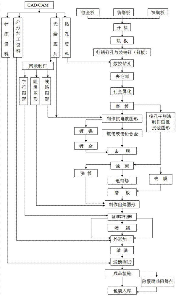
[0023] A small-pitch P2.5 double-layer circuit board manufacturing process of the present invention comprises the following steps,

[0024] S1: Print the PCB diagram of the light side and the driving side of the small-pitch P2.5 double-layer circuit board to be produced on the thermal transfer paper by laser printer or inkjet printer;

[0025] S2: Stick the printed bottom layer drawing on the copper clad laminate with paper tape, wherein the lamp surface is glued to the bottom layer, the driving surface is glued to the top layer, and positioning holes are drilled on the copper clad laminate;

[0026] S3: Adsorb the toner on the thermal transfer paper to the copper clad board through the thermal transfer machine;

[0027] S4: Wash off the excess copper clad, and complete the production of the small-pitch P2.5 double-layer circuit board. ...


PUM


Abstract

The invention relates to a small spacing P2.5 double-layer circuit board manufacturing process. This method comprises the steps that 1, a PCB graph of a lamp face of a small spacing P2.5 double-layer circuit board to be manufactured and a PCB graph of a driving face of the small spacing P2.5 double-layer circuit board to be manufactured are printed on heat transfer paper through a laser printer or an ink-jet printer separately; 2, printed bottom-layer drawing paper is attached to a copper-clad plate by a paper self-adhesive tape, wherein the lamp face is attached to a bottom layer, the driving face is attached to a top layer, and positioning holes are drilled in the copper-clad plate; 3, ink powder is absorbed on the copper-clad plate through a heat transfer machine; 4, extra clad copper is washed off, and manufacturing of the small spacing P2.5 double-layer circuit board is finished. According to the small spacing P2.5 double-layer circuit board manufacturing process, a four-layer plate of an existing small spacing P2.5 double-layer circuit board is changed to a double-layer plate, the problems which exist in the prior art of small spacing P2.5 double-layer circuit boards are alleviated that the technology is cumbersome, high-frequency signals are attenuated and the production cost is high.

Description

technical field [0001] The invention belongs to the field of lighting products, and in particular relates to a small-pitch P2.5 double-layer circuit board manufacturing process. Background technique [0002] The small-pitch P2.5 modules currently on the market generally use multi-layer board technology, and most of them are 4-layer boards. The small-pitch P2.5 module of this application uses double-sided panels. [0003] The small-pitch P2.5 modules on the market are commonly 4-layer boards. In order to obtain good-quality etching patterns, it is necessary to ensure that the resist layer is firmly bonded to the substrate surface, and the substrate surface is required to be free of oxide layers, oil, and dust. , fingerprints and other dirt. Therefore, before coating the resist layer, it is first necessary to clean the surface of the board and make the surface of the copper foil reach a certain degree of roughness. Inner layer board: start to make a four-layer board, and th...

Claims


Application Information

Patent Timeline
IPC IPC(8): H05K3/20
CPCH05K3/207H05K2203/0531
Inventor 林春仁檀灵真
Owner FUJIAN XIANGYUN PHOTOELECTRIC TECH
Learn More