An epitaxial structure of an avalanche diode and a method for manufacturing the avalanche diode

An avalanche diode and epitaxial structure technology, which is applied in semiconductor/solid-state device manufacturing, thyristors, semiconductor devices, etc., can solve the problems of difficulty in improving the yield rate of avalanche diode devices, poor uniformity of epitaxial thickness, and increasing the difficulty of control circuits, etc.

Active Publication Date: 2019-05-07
武汉光谷量子技术有限公司
View PDF5 Cites 0 Cited by
  • Summary
  • Abstract
  • Description
  • Claims
  • Application Information

AI Technical Summary

Problems solved by technology

When the thickness of the avalanche gain layer is not uniform, the operating characteristics of each device will be significantly different, resulting in differences in operating characteristics between devices, and increasing the difficulty of control circuit design, making it difficult to improve the yield of manufactured avalanche diode devices
Especially when the thickness uniformity of epitaxy is not good, the yield rate of high-frequency avalanche diode devices can be lower than 20%.

Method used


Image

  • An epitaxial structure of an avalanche diode and a method for manufacturing the avalanche diode
  • An epitaxial structure of an avalanche diode and a method for manufacturing the avalanche diode
  • An epitaxial structure of an avalanche diode and a method for manufacturing the avalanche diode

Examples


Embodiment Construction

[0021] The present invention will be described in further detail below in conjunction with the accompanying drawings and embodiments.

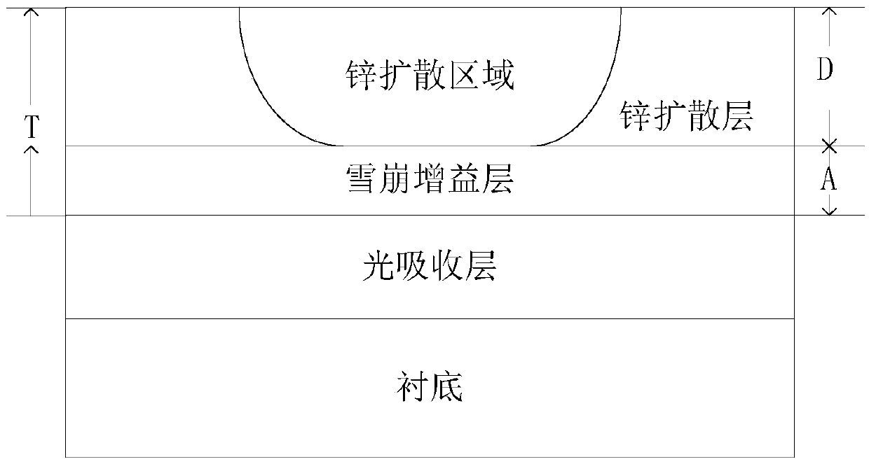
[0022] see figure 1 As shown, the embodiment of the present invention provides an epitaxial structure of an avalanche diode, including a substrate, a light absorbing layer is formed above the substrate, an avalanche gain layer is formed above the light absorbing layer, and a zinc diffusion layer is formed above the avalanche gain layer. Floor. The zinc diffusion layer is made of InP material, and the avalanche gain layer is made of In 0.52 Al 0.48 As material, In x Ga (1-x) As y P (1-y) Material, In x Ga y Al (1-x-y) As material, In x Ga (1-x) As y P (1-y) Composition of Gradient Material or In x Ga y Al (1-x-y) The composition of As is composed of graded materials, where In x Ga (1-x) As y P (1-y) Material or In x Ga (1-x) As y P (1-y) 0x Ga y Al (1-x-y) As material or In x Ga y Al (1-x-y) In the composition gradi...


PUM


Abstract

The present invention discloses an epitaxial structure of an avalanche diode, and relates to the technical field of semiconductor manufacturing. The epitaxial structure of the avalanche diode comprises a substrate. A light-absorbing layer is formed above the substrate. An avalanche gain layer is formed above the light-absorbing layer. A zinc diffusion layer is formed above the avalanche gain layer. The zinc diffusion layer is made of the InP material. The avalanche gain layer is made of component-gradient materials composed of the In0.52Al0.48As material, the InxGa(1-x)AsyP(1-y) material, the InxGayAl(1-x-y)As mateiral and the InxGa(1-x)AsyP(1-y) material, or component-gradient materials composed of InxGayAl(1-x-y)As. In the InxGa(1-x)AsyP(1-y) material or the component-gradient material of InxGa(1-x)AsyP(1-y), x is larger than 0 and smaller than 1, and y is larger than 0 and smaller than 1. In the InxGayAl(1-x-y)As material or the component-gradient material of InxGayAl(1-x-y)As, x is larger than 0 and smaller than 1, y is larger than 0 and smaller than 1 and the sum of x+y is larger than 0 and smaller than 1. According to the technical scheme of the invention, the depth of the zinc diffusion area is effectively controlled, and the thickness of the avalanche gain layer is accurately controlled. The yield of avalanche diode devices is improved. The invention also discloses an avalanche diode manufacturing method.

Description

technical field [0001] The invention relates to the technical field of semiconductor manufacturing, in particular to an epitaxial structure of an avalanche diode and a method for manufacturing the avalanche diode. Background technique [0002] When manufacturing high-frequency response avalanche diodes (Avalanche Photodiodes: APD), if a planar structure design is adopted, it is generally necessary to use zinc diffusion technology to define the receiving area of ​​the device. The receiving area of ​​this device is usually equal to the area of ​​zinc diffusion. size. For avalanche diode devices with high frequency response, it is necessary to precisely control the thickness of the avalanche gain layer to achieve the best device operation characteristics, especially the frequency response of the device. refer to figure 1 As shown, the upper layer of the light-absorbing layer of the avalanche diode is generally made of low-doped InP material, and its total thickness is T (gene...

Claims


Application Information

Patent Timeline
Patent Type & Authority Patents(China)
IPC IPC(8): H01L29/861H01L21/329H01L29/06
CPCH01L29/0626H01L29/66113H01L29/861
Inventor 黄文勇王肇中
Owner 武汉光谷量子技术有限公司
Why Eureka
Try Eureka