Method for generating solid modulation plasma photonic crystals with three refractive indexes
A kind of plasma, photonic crystal technology, applied in the field of plasma application technology and optics
- Summary
- Abstract
- Description
- Claims
- Application Information
AI Technical Summary
Problems solved by technology
Method used
Image


Examples
Embodiment 1
[0023] Example 1, a device for producing a solid-modulated plasmonic photonic crystal with three refractive indices.
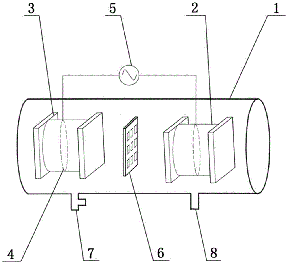
[0024] Such as figure 1 As shown, the device used in the present invention is specifically: two airtight dielectric containers are symmetrically arranged in a horizontal cylindrical vacuum reaction chamber 1, and water is injected into the airtight dielectric container to form two opposite water electrodes. 2. The two water electrodes 2 are electrically connected with the plasma generating power source 5 outside the vacuum reaction chamber 1 . In this embodiment, the water electrode 2 is made of a plexiglass tube sealed by glass baffles 3 at both ends, the plexiglass tube is filled with water, and a copper ring 4 is set in the plexiglass tube. The two copper rings 4 are respectively electrically connected to the positive pole and the negative pole of the plasma generation power supply 5 through power lines. The thickness of the glass block 3 is between 1.5 ...
Embodiment 2
[0031] combine figure 1 and figure 2 , a vacuum reaction chamber 1 is set, an air inlet 7 and an air outlet 8 are opened on the wall of the vacuum reaction chamber 1, and two water electrodes 2 opposite to each other are installed in the vacuum reaction chamber 1. The water electrode 2 is composed of a plexiglass tube sealed with glass baffles 3 on both sides and filled with water, and a built-in copper ring 4 is electrically connected to the plasma generating power supply 5 outside the vacuum reaction chamber 1 .
[0032] A solid frame 6 with a thickness of 2mm is arranged between the two water electrodes 2, the solid frame 6 is an acrylic plate, the plane where it is located is perpendicular to the axes of the two water electrodes 2, and the two sides are close to the two water electrodes 2 end face. Nine square through holes 6 - 1 with equal size and side length of 8 mm are opened in the inner area of the solid frame 6 , and the nine square through holes 6 - 1 are arra...
Embodiment 3
[0038] Compared with Embodiment 2, this embodiment differs in that: discharge gas pressure P=0.15atm, voltage amplitude U=3.2kV.
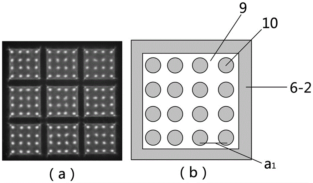
[0039] see Figure 5 , the present embodiment is produced by solid (solid edge 6-2 with a width of 2mm), gas (that is, the gas in the second undischarged region 12) and a lattice constant of а 2 The photo of the solid modulated plasmonic photonic crystal formed by the periodic arrangement of the quadrilateral second plasma 13 (taken by a common camera) as Figure 5 (a), Figure 5 A partial schematic diagram of a cycle in (a) as Figure 5 (b) shown. Figure 5 The gas shown in (b) (that is, the gas in the second undischarged region 12), the second plasma 13, and the solid edge 6-2 have different refractive indices, wherein the refractive index of the gas is 1; the second plasma 13 The refractive index of the solid edge 6-2 is less than 1; the refractive index of the solid edge 6-2 is between 1.2 and 1.4. This example also produces solid-modulate...
PUM
 Abstract
Description
Claims
Application Information
 - R&D
- Intellectual Property
- Life Sciences
- Materials
- Tech Scout
- Unparalleled Data Quality
- Higher Quality Content
- 60% Fewer Hallucinations
Browse by: Latest US Patents, China's latest patents, Technical Efficacy Thesaurus, Application Domain, Technology Topic, Popular Technical Reports.
© 2025 PatSnap. All rights reserved.Legal|Privacy policy|Modern Slavery Act Transparency Statement|Sitemap|About US| Contact US: help@patsnap.com