Dual-gate thin film transistor and preparation method therefor, array substrate and display apparatus
A technology of thin film transistors and array substrates, which is applied in the fields of double-gate thin film transistors and their preparation, array substrates and display devices, can solve problems such as poor stability, and achieve the effects of increased production capacity, simple structure, and simplified manufacturing process steps
- Summary
- Abstract
- Description
- Claims
- Application Information
AI Technical Summary
Problems solved by technology
Method used
Image
Examples
Embodiment 1
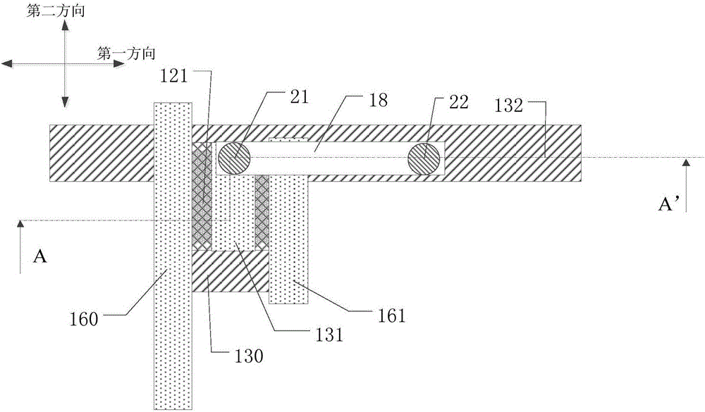
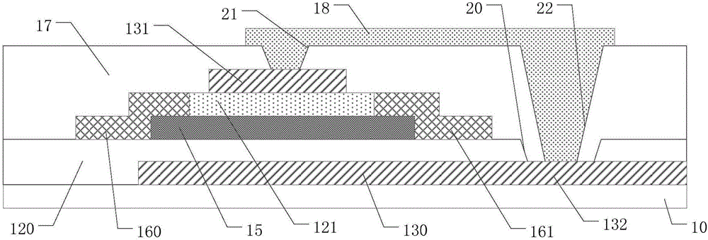
[0047] Figure 1a The plan view of shows the plan view of the dual-gate thin film transistor provided in this embodiment, Figure 1b for along Figure 1a Schematic diagram of the cross-sectional structure of the double-gate thin film transistor taken along the line A-A'.
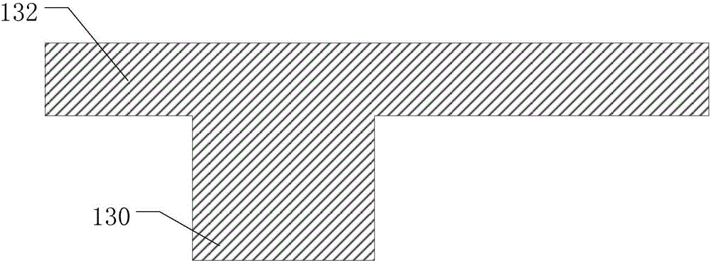
[0048] Such as Figure 1a and Figure 1b As shown, the double-gate thin film transistor of this embodiment includes a base substrate 10; a first gate 130 is disposed on the base substrate 10; a first gate insulating layer 120 is disposed on the first gate 130, so The first gate insulating layer 120 includes a first via hole 20 exposing a part of the first gate 130; the active layer 15 is disposed on the first gate insulating layer 120, and the active layer 15 is connected to the first gate insulating layer 130. A gate 130 is at least partially overlapped in a direction perpendicular to the base substrate 10; the second gate insulating layer 121 is disposed on the active layer 15; the first electrode 160 and...
Embodiment 2
[0079] Figure 3a shows a plan view of the double-gate thin film transistor provided in Embodiment 2, Figure 3b for along Figure 3a A cross-sectional view of a double-gate thin film transistor taken along the middle line B-B'. Such as Figure 3a and 3b As shown, in the double-gate thin film transistor provided in this embodiment, the second gate insulating layer 122 completely covers the active layer 15, and the second gate 131, the first electrode 162 and the second electrode 163 are formed on the on the second gate insulating layer 122 . The second gate insulating layer 122 includes a fourth via hole 23 , a fifth via hole 24 , and a sixth via hole 25 exposing the first via hole 20 , which expose at least a part of the active layer 15 and are respectively located on both sides of the second gate 131 . The first electrode 162 is electrically connected to the active layer 15 through the fourth via hole 23, and the second electrode 163 is electrically connected to the act...
Embodiment 3
[0082] Figure 4a shows a plan view of the double-gate thin film transistor provided in Embodiment 3, Figure 4b for along Figure 4a A cross-sectional view of a double-gate thin film transistor taken along the middle line C-C'. In Embodiment 1 and Embodiment 2, the connection electrode 18 is disposed on the first passivation layer 17. In this embodiment, as Figure 4a and 4bAs shown, the connection electrode 180 is disposed on the second gate insulating layer 123 , and the connection electrode 180 is lap connected to the second gate 131 and electrically connected to the gate line 132 through the first via hole 20 . In this embodiment, the first passivation layer 17 is omitted, and the second gate insulating layer 123 is used to insulate the connecting electrode 180, the active layer 15, and the second electrode 165, thereby further reducing the number of film layers and simplifying the manufacturing process steps. Reduce production costs and effectively increase productio...
PUM
 Abstract
Description
Claims
Application Information
 - Generate Ideas
- Intellectual Property
- Life Sciences
- Materials
- Tech Scout
- Unparalleled Data Quality
- Higher Quality Content
- 60% Fewer Hallucinations
Browse by: Latest US Patents, China's latest patents, Technical Efficacy Thesaurus, Application Domain, Technology Topic, Popular Technical Reports.
© 2025 PatSnap. All rights reserved.Legal|Privacy policy|Modern Slavery Act Transparency Statement|Sitemap|About US| Contact US: help@patsnap.com


